RP2040 UART in Baremetal
In this article, we will discuss how to use the UART on RP2040 in a bare metal application.
Paspberry Pi Pico, RP2040, ARM, Cortex M0+, Baremetal, UART, Serial communication, MCU
--by Captdam @ May 20, 2026Index
This article is intended for developers who are familiar with 8-bit MCUs and use Assembly and C language to develop bare metal applications, but new to 32-bit RP2040 and ARM Cortex-M0+.
Since we are creating bare metal applications, we will be directly writing to and reading from the MCU control registers. No library is used.
We will rely on the documents heavily. It includes all information we need about the MCU control registers.
Because of the RP2040 document updates, and for some reason they decided to redirect my links to the old document to the new document, I decided to create a copy of the current version (2025-02-20) on my server. You may obtain this document from the official link here (as 2026-02-10).
In this article, we will discuss how to use the UART on RP2040 in a bare metal application.
We will concluding all topics we discussed in the previous articles:
- Using the SDK bootloader to execute (the 3rd stage bootloader) from flash. See W25Q Flash and RP2040 SDK Bootloader in Baremetal.
- Launch core 1 from core 0. See RP2040 Baremetal Dual-core Application and Core 1 Launch Protocol.
- Switch the system clock source from ROSC to 132MHz PLL. See Switch RP2040 Clock Source in Baremetal: ROSC, XOSC and PLL.
- Copy program and data from flash (for storage) to SRAM (to avoid flash cache miss). See Compare RP2040 Executable Memory Regions and Load Program From Flash into SRAM.
- Manual linking the program from binary object files, Assembly code files and C language code files.
We will create a simple dual-core baremetal program that:
- Core 0 setup the UART.
- Core 0 will receive a word from the PC via UART.
- Core 0 sends the received word to core 1.
- Core 1 modifies the received word by adding 1 to its ASCII code. For example, A + 1 is B.
- Core 1 sends the modified word and other messages to the PC via UART.
Project file for RP2040 UART in Baremetal can be found here.
Linking Script and Compile Commands (Review)
Let's review what we did in previous articles to compile and link the programs:
Compile
arm-none-eabi-as --warn --fatal-warnings -g *.s -o s.o
arm-none-eabi-objdump --disassembler-options=force-thumb -Dxs s.o > s.list

arm-none-eabi-gcc -mcpu=cortex-m0plus -c -O3 *.c -o c.o
arm-none-eabi-objdump --disassembler-options=force-thumb -Dxs c.o > c.list

arm-none-eabi-ld -nostdlib -nostartfiles -T main.ld *.o -o main.elf
arm-none-eabi-objdump --disassembler-options=force-thumb -dxs main.elf > main.list
pico-elf2uf2 main.elf main.uf2
These commands will:
- Assemble all assembly code files (.s) into object file
s.o. - Compile (but do not link) all C language code files (.c) into object file
c.o. - Link all object files into elf file
main.elfaccording to linker scriptmain.ld. This includes not only the two object file we just created from assembly and C language source code, but also pre-generated object files in the working directory, such as the SDK bootloader (boot2.o). - Generate the uf2 file
main.uf2from the elf filemain.elf, that can be downloaded to RP2040 via USB.
Linking
MEMORY {
	FLASH(rwx) : ORIGIN = 0x10000000, LENGTH = 2048k
	SRAM(rwx) : ORIGIN = 0x20000000, LENGTH = 256k
	SRAM_4(rwx) : ORIGIN = 0x20040000, LENGTH = 4k
	SRAM_5(rwx) : ORIGIN = 0x20041000, LENGTH = 4k
	SRAM_0(rwx) : ORIGIN = 0x21000000, LENGTH = 64k
	SRAM_1(rwx) : ORIGIN = 0x21010000, LENGTH = 64k
	SRAM_2(rwx) : ORIGIN = 0x21020000, LENGTH = 64k
	SRAM_3(rwx) : ORIGIN = 0x21030000, LENGTH = 64k
}

ENTRY(_boot_start)

SECTIONS {
	.boot : {
		*(.boot2)
		*(.boot3)
	} > FLASH
	_boot_start = ORIGIN(FLASH);
	_boot_end = _boot_start + SIZEOF(.boot);

	.core0 : {
		. = ALIGN (256);
		*(.c0_vector)
		*(.c0_data)
		*(.c0_text)
	} > SRAM_4 AT > FLASH
	_core0_dest = ORIGIN(SRAM_4);
	_core0_start = _boot_end;
	_core0_end = _core0_start + SIZEOF(.core0);

	.core1 : {
		. = ALIGN (256);
		*(.c1_vector)
		*(.c1_data)
		*(.c1_text)
	} > SRAM_5 AT > FLASH
	_core1_dest = ORIGIN(SRAM_5);
	_core1_start = _core0_end;
	_core1_end = _core1_start + SIZEOF(.core1);

	.unspecified : {
		*(.text)
		*(.data)
		*(.bss)
	}
	ASSERT(!(SIZEOF(.unspecified)), "Unspecified text, data, and/or bss section")
}
We had discussed this linker script in my previous article: Compare RP2040 Executable Memory Regions and Load Program From Flash into SRAM. In conclusion:
- Place the SDK 2nd stage bootloader in the beginning of flash (address 0x10000000), followed by our 3rd stage bootloader.
- Then, place contents of core 0 in flash, vector table
.c0_vectorfirst (so it can be 256-byte aligned after loading into SRAM), followed by data.c0_dataand program instruction.c0_text. Assign them the address of SRAM bank 4 (0x20040000). - Next, place contents of core 1 in flash, vector table
.c1_vectorfirst, followed by data.c1_dataand program instruction.c1_text. Assign them the address of SRAM bank 5 (0x20041000).
Bootloader (Review)
Now, let's review the two bootloaders we used in this program.
SDK 2nd Stage Bootloader - boot2.o
We will copy the pre-generated SDK 2nd stage bootloader from the previous article: W25Q Flash and RP2040 SDK Bootloader in Baremetal.
In conclusion, this bootloader:
- Must be placed at the beginning of the flash at address 0x10000000 and must be 256-byte in size, as required by the on-chip 1st stage bootloader.
- Configure the SSI XIP (to map the external flash into the internal XIP memory space) to allow the CPUs to directly read from external flash.
- Launch the user code (which is our 3rd stage bootloader) which is placed immediately after the SDK 2nd stage bootloader.
Our 3rd Stage Bootloader - boot3.o
We will copy the pre-generated 3rd stage bootloader from the previous article: Compare RP2040 Executable Memory Regions and Load Program From Flash into SRAM.
In conclusion, this bootloader:
- Start the crystal oscillator XOSC that is more accurate than the default ring oscillator ROSC.
- Use XOSC as the reference clock source to start the system PLL, which runs at 132MHz. Then, switch the system clock source to the system PLL.
- Copy the program (vector tables, data and instruction) from flash (for storage) to SRAM (to avoid flash cache miss). Place core 0's content in SRAM bank 4, address 0x20040000, core 1's content in SRAM bank 5, address 0x20041000.
- Launch core 1, use SRAM bank 5 for stack. Start core 0, use SRAM bank 4 for stack.
Assembly Code File
.cpu cortex-m0plus
.thumb
.align 2
.thumb_func
In this program, we will not use any assembly language code. However, we have to create an "empty" assembly code file just to satisfy the compile commands.
C Language File - Vector Table
Table Structure
Let's define the vector table first. The same table structure applied to both cores.
The first 16 vectors are required by ARM Cortex M0+ CPU.
Followed by a set of IRQ service routine addresses. This is implementation dependent because different implementations can have different peripherals. Details can be found in the RP2040 document.
We can create a header file vector.h to store the address of each vector:
#define vector_sp			0
#define vector_reset		1
#define vector_nmi		2
#define vector_hardfault	3
#define vector_svcall		11
#define vector_pendsv		14
#define vector_systick		15
#define vector_irq(n)		(16 + n)

#define irq_timer0		0
#define irq_timer1		1
#define irq_timer2		2
#define irq_timer3		3
#define irq_pwmwrap		4
#define irq_usbctrl		5
#define irq_xip			6
#define irq_pio00			7
#define irq_pio01			8
#define irq_pio10			9
#define irq_pio11			10
#define irq_dma0			11
#define irq_dma1			12
#define irq_io_bank0		13
#define irq_io_qspi		14
#define irq_sio_proc0		15
#define irq_sio_proc1		16
#define irq_clocks		17
#define irq_spi0			18
#define irq_spi1			19
#define irq_uart0			20
#define irq_uart1			21
#define irq_adc			22
#define irq_i2c0			23
#define irq_i2c1			24
#define irq_rtc			25
Vector Table Code
In this example, we only specify the first vector for initial SP and the second vector for entry point:
uint32_t c0_vector[48] __attribute__((section(".c0_vector"))) = {
	[vector_sp] = 0x20041000,
	[vector_reset] = (uint32_t)c0_reset
};

uint32_t c1_vector[48] __attribute__((section(".c1_vector"))) = {
	[vector_sp] = 0x20042000,
	[vector_reset] = (uint32_t)c1_reset
};
Note that in C, the compiler will set the Thumb-bit (the LSB of the address) for us.
We will create the vector tables for both core 0 and core 1. Place the vector table for core 0 in section .c0_vector and the vector table for core 1 in section .c1_vector. This helps us to specify the addresses of the vector tables in the linking stage.
| Vector | Core 0 | Core 1 |
|---|---|---|
| Initial SP | Top of SRAM bank 4 (0x20041000) | Top of SRAM bank 5 (0x20042000) |
| Entry point | Function c0_reset |
Function c1_reset |
C Language File - Program on Core 0
Now, let's define the program running on core 0:
__attribute__((long_call)) extern void boot3_clearInterprocessorMailboxRx();

void c0_reset() __attribute__((section(".c0_text"))) __attribute__((naked));

void c0_reset() {
	(boot3_clearInterprocessorMailboxRx + 1)();
Define the entry point for core 0, function c0_reset.
This function will never return; therefore, it is not necessary to preserve the calling stack. We can make it naked, this tells the compiler to not generate code that preserves the calling stack.
Place this function in section .c0_text.
Before we perform any actual operations, we want to empty the inter-processor mailbox that may be contaminated during core 1 launch protocol. To do so, we will call the function boot3_clearInterprocessorMailboxRx, saved in boot3.o.
Because boot3_clearInterprocessorMailboxRx is stored in flash but c0_reset is running in SRAM, the distance between them is greater than 16MiB. We have to declare that function lang_call. By default, the compiler uses the convenient bl offset instruction, which can only be used for short calls with limited distance between the caller and the callee. Note that, at compile time (before linking), the compiler deesn't know the address of the caller and callee. For long calls, we must load the callee's address into a register, then execute the bx r instruction.
Furthermore, when calling the function, we must manually add 1 to the callee function's address because it is a Thumb function. The compiler does not automatically set the Thumb bit for us in this case. This is because at compile time, the compiler doesn't know the external function is a Thumb or ARM function.
C Macro
We will create a header file reg.h to store the address of each control register. This helps clearfy our C source code file.
#define reg(reg_name)		(*(uint32_t volatile * const)(reg_name))
#define reg_xor(reg_name)	(*(uint32_t volatile * const)(reg_name + 0x1000))
#define reg_set(reg_name)	(*(uint32_t volatile * const)(reg_name + 0x2000))
#define reg_clr(reg_name)	(*(uint32_t volatile * const)(reg_name + 0x3000))
Recall that, the AHB-Lite Crossbar supports atomic register access. To do so, add an offset to the register address.
Configure the Peripherals
To use the UART to receive and send data, we must enable it first. To do so, we will need to:
Reset
#define reg_resets_reset			0x4000c000
#define reg_resets_reset_usbctrl		24
#define reg_resets_reset_uart1		23
#define reg_resets_reset_uart0		22
#define reg_resets_reset_timer		21
#define reg_resets_reset_tbman		20
#define reg_resets_reset_sysinfo		19
#define reg_resets_reset_syscfg		18
#define reg_resets_reset_spi1			17
#define reg_resets_reset_spi0			16
#define reg_resets_reset_rtc			15
#define reg_resets_reset_pwm			14
#define reg_resets_reset_pll_usb		13
#define reg_resets_reset_pll_sys		12
#define reg_resets_reset_pio1			11
#define reg_resets_reset_pio0			10
#define reg_resets_reset_pads_qspi		9
#define reg_resets_reset_pads_bank0		8
#define reg_resets_reset_jtag			7
#define reg_resets_reset_io_qspi		6
#define reg_resets_reset_io_bank0		5
#define reg_resets_reset_i2c1			4
#define reg_resets_reset_i2c0			3
#define reg_resets_reset_dma			2
#define reg_resets_reset_busctrl		1
#define reg_resets_reset_adc			0
	reg_clr(reg_resets_reset)
		= (1<<reg_resets_reset_io_bank0)
		| (1<<reg_resets_reset_uart0);
Bring GPIO bank 0 and UART0 out of reset. Note we used the atomic clear operation to prevent unintended reset of other functionalities.
GPIO Function
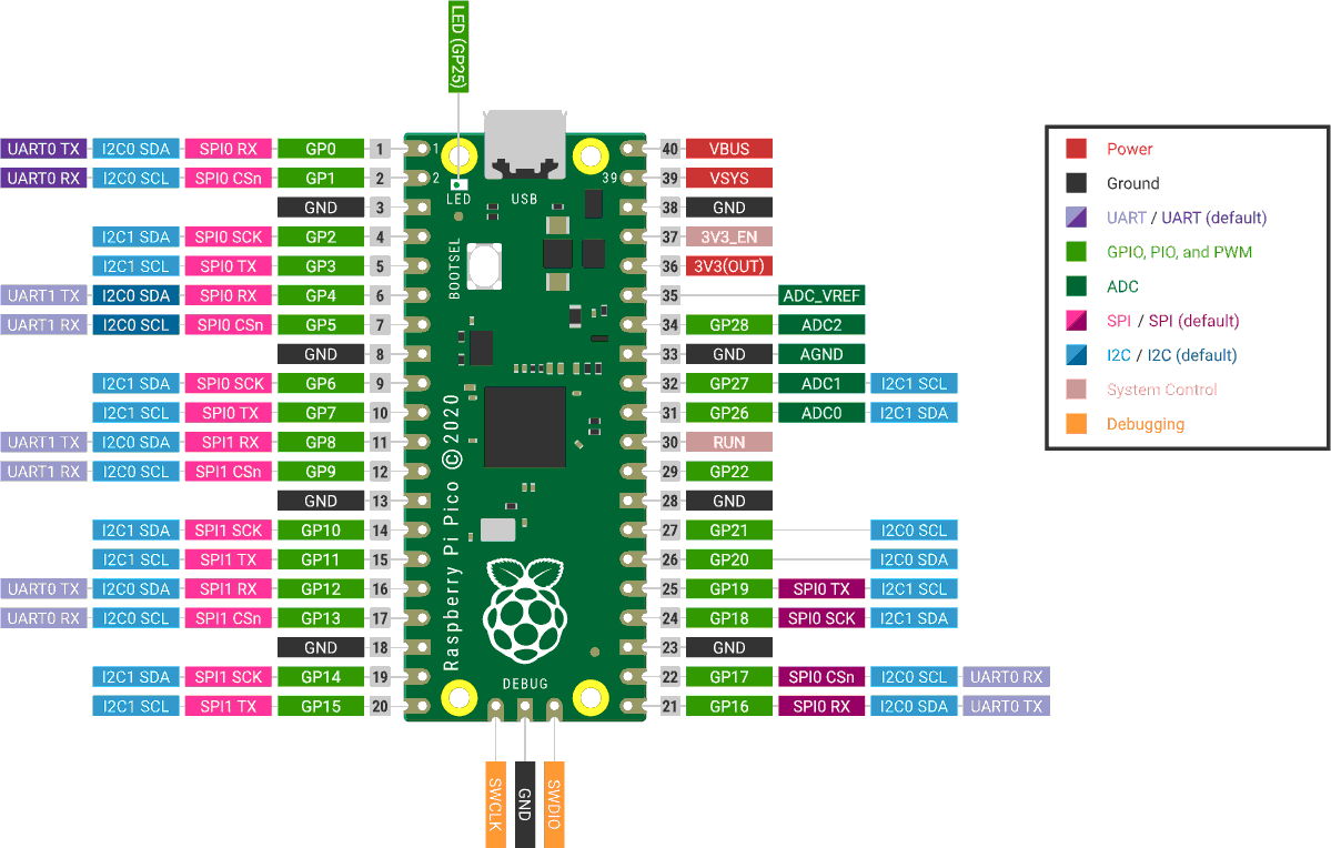
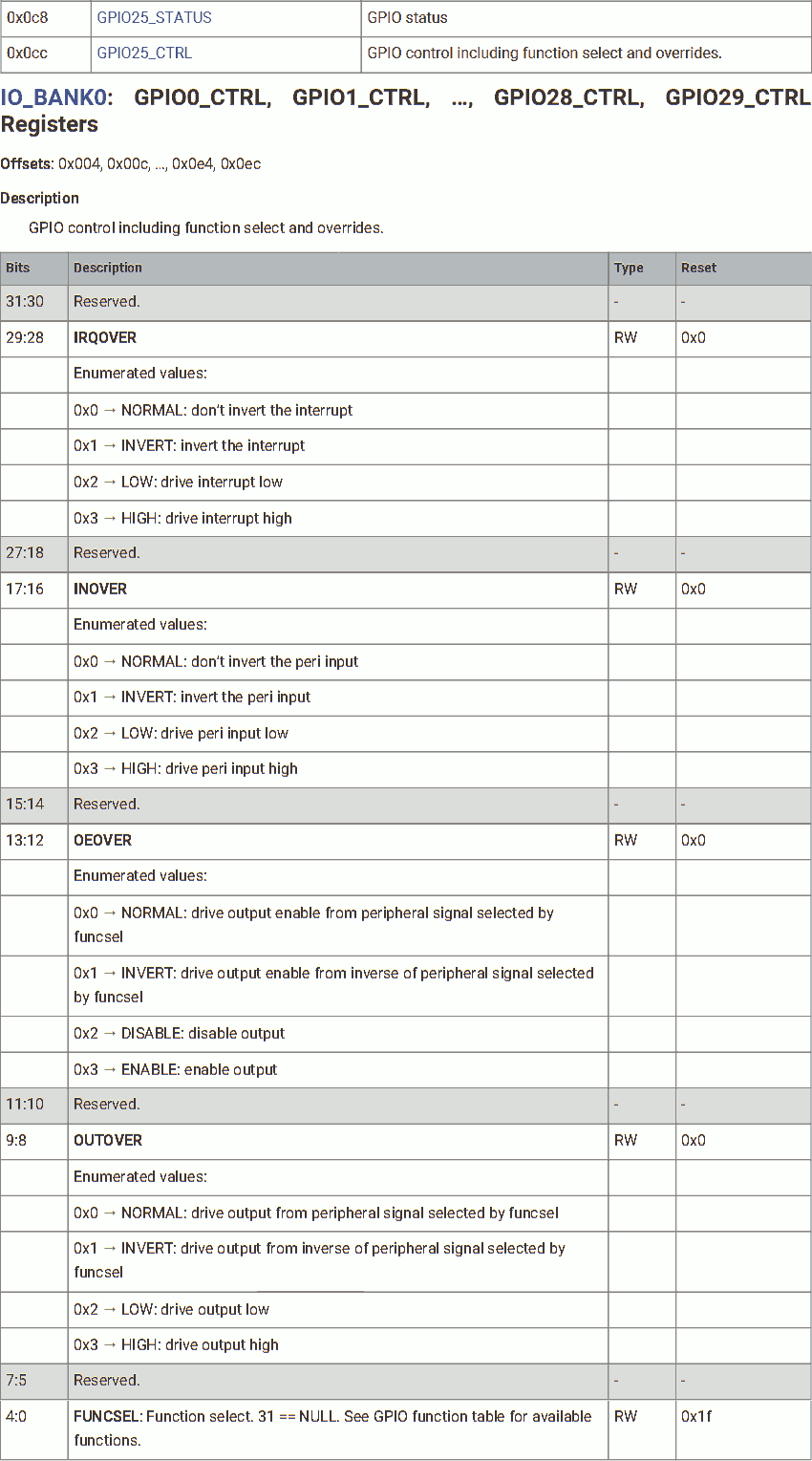
#define reg_io_bank0_gpio_ctrl(io) (0x40014004 + 8 * io)
#define reg_io_bank0_gpio_ctrl_irqover 29
#define reg_io_bank0_gpio_ctrl_irqover_normal 0
#define reg_io_bank0_gpio_ctrl_irqover_invert 1
#define reg_io_bank0_gpio_ctrl_irqover_low 2
#define reg_io_bank0_gpio_ctrl_irqover_high 3
#define reg_io_bank0_gpio_ctrl_inover 16
#define reg_io_bank0_gpio_ctrl_inover_normal 0
#define reg_io_bank0_gpio_ctrl_inover_invert 1
#define reg_io_bank0_gpio_ctrl_inover_low 2
#define reg_io_bank0_gpio_ctrl_inover_high 3
#define reg_io_bank0_gpio_ctrl_oeover 12
#define reg_io_bank0_gpio_ctrl_oeover_normal 0
#define reg_io_bank0_gpio_ctrl_oeover_invert 1
#define reg_io_bank0_gpio_ctrl_oeover_low 2
#define reg_io_bank0_gpio_ctrl_oeover_high 3
#define reg_io_bank0_gpio_ctrl_outover 8
#define reg_io_bank0_gpio_ctrl_outover_normal 0
#define reg_io_bank0_gpio_ctrl_outover_invert 1
#define reg_io_bank0_gpio_ctrl_outover_low 2
#define reg_io_bank0_gpio_ctrl_outover_high 3
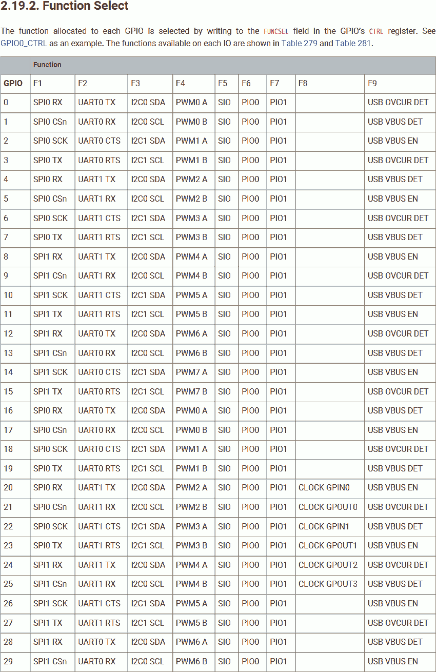
#define reg_io_bank0_gpio_ctrl_funcsel 0
#define reg_io_bank0_gpio_ctrl_spi 1
#define reg_io_bank0_gpio_ctrl_uart 2
#define reg_io_bank0_gpio_ctrl_i2c 3
#define reg_io_bank0_gpio_ctrl_pwm 4
#define reg_io_bank0_gpio_ctrl_sio 5
#define reg_io_bank0_gpio_ctrl_pio0 6
#define reg_io_bank0_gpio_ctrl_pio1 7
#define reg_io_bank0_gpio_ctrl_clock 8
#define reg_io_bank0_gpio_ctrl_usb 9
	reg(reg_io_bank0_gpio_ctrl(0))
		= (reg_io_bank0_gpio_ctrl_uart<<reg_io_bank0_gpio_ctrl_funcsel);
	reg(reg_io_bank0_gpio_ctrl(1))
		= (reg_io_bank0_gpio_ctrl_uart<<reg_io_bank0_gpio_ctrl_funcsel);
Set the function of GPIO 0 and 1 to UART.
Peripheral Clock
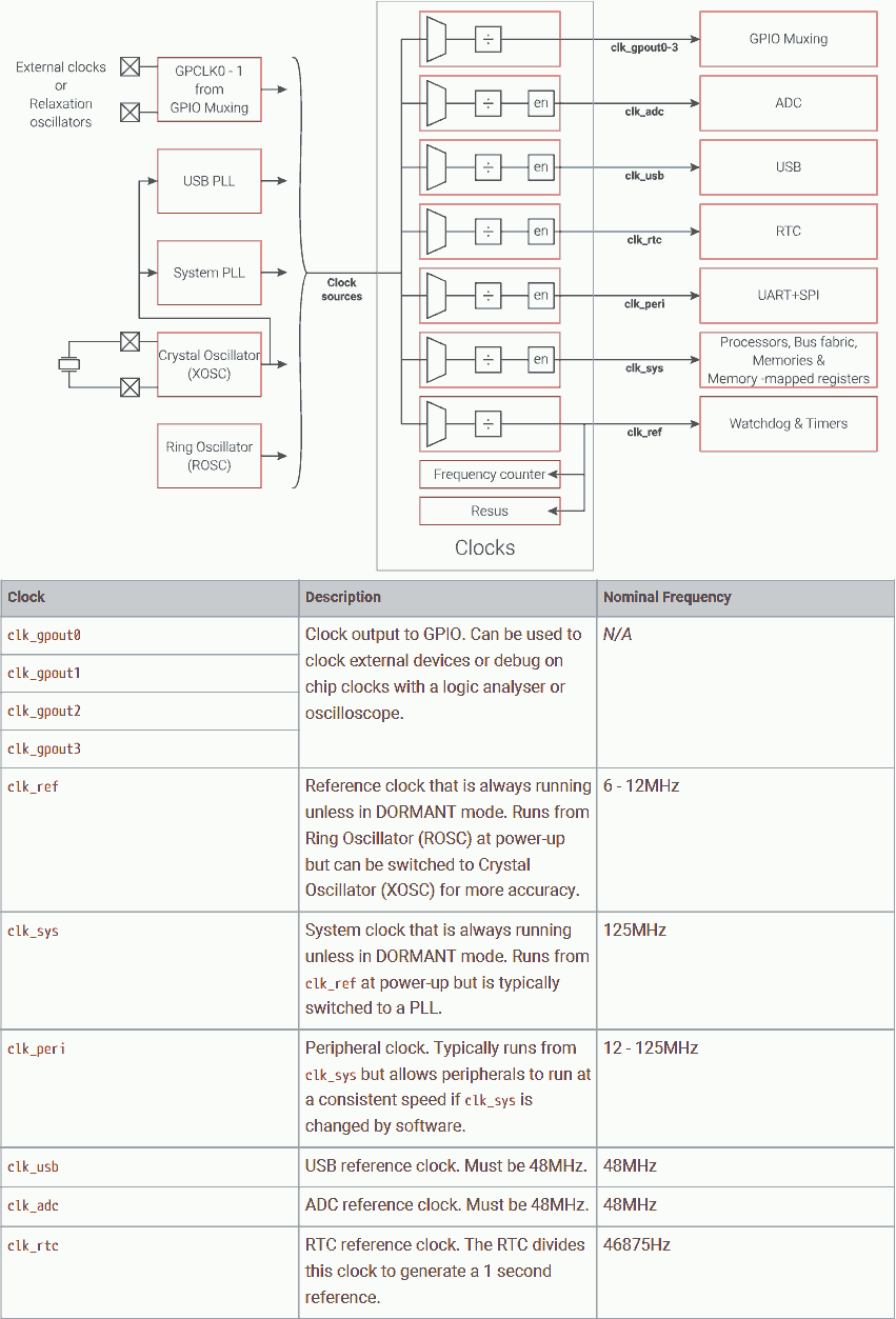
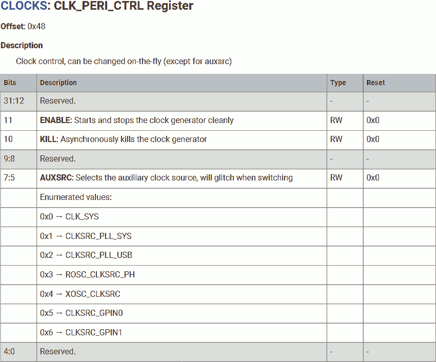
#define reg_clk_peri_ctrl			0x40008048
#define reg_clk_peri_en				11
#define reg_clk_peri_kill			10
#define reg_clk_peri_auxsrc			5
#define reg_clk_peri_auxsrc_sys		0
#define reg_clk_peri_auxsrc_syspll		1
#define reg_clk_peri_auxsrc_usbpll		2
#define reg_clk_peri_auxsrc_roscph		3
#define reg_clk_peri_auxsrc_xosc		4
#define reg_clk_peri_auxsrc_gpin0		5
#define reg_clk_peri_auxsrc_gpin1		6
	reg(reg_clk_peri_ctrl)
		= (1<<reg_clk_peri_en)
		| (reg_clk_peri_auxsrc_sys<<reg_clk_peri_auxsrc);
The peripheral clock is used to drive UART and it is disabled by default. We need to enable it before we can use the UART. We will use the system clock (which uses system PLL as input) to drive the peripheral clock, clocked at 132MHz.
Note the peripheral clock uses AUX MUX which generates glitch when switched and it requires 2 clock cycles to stop and 2 clock cycles to restart.
In general, we should disable any device that relies on this clock source when switching. Because the MCU just start, we are sure there is no device using this clock.
UART Configuration - BAUD
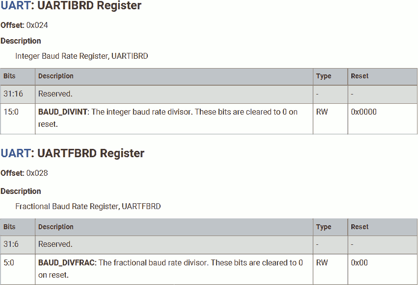
#define reg_uart_uartibdr(n)		(0x40034024 + 0x4000 * n)
#define reg_uart_uartfbdr(n)		(0x40034028 + 0x4000 * n)
There are two sets of UART in RP2040. Base address of UART0 is 0x40034000, base address of of UART1 is 0x40038000.
	reg(reg_uart_uartibdr(0)) = 859;
	reg(reg_uart_uartfbdr(0)) = 24;
First, set the BAUD rate. Because the system is clocked at 132MHz and our PC expects the UART signal at 9600 BAUD, the UART clock divisor should be:
132MHz / 9600BAUD / 16 = 859.375
where the integer part is 859.
The UART clock divisor allows 6-bit fractional part, which means:
0.375 * (2^6) = 0.375 * 64 = 24
where the fractional part should be 24.
UART Configuration - Line Control
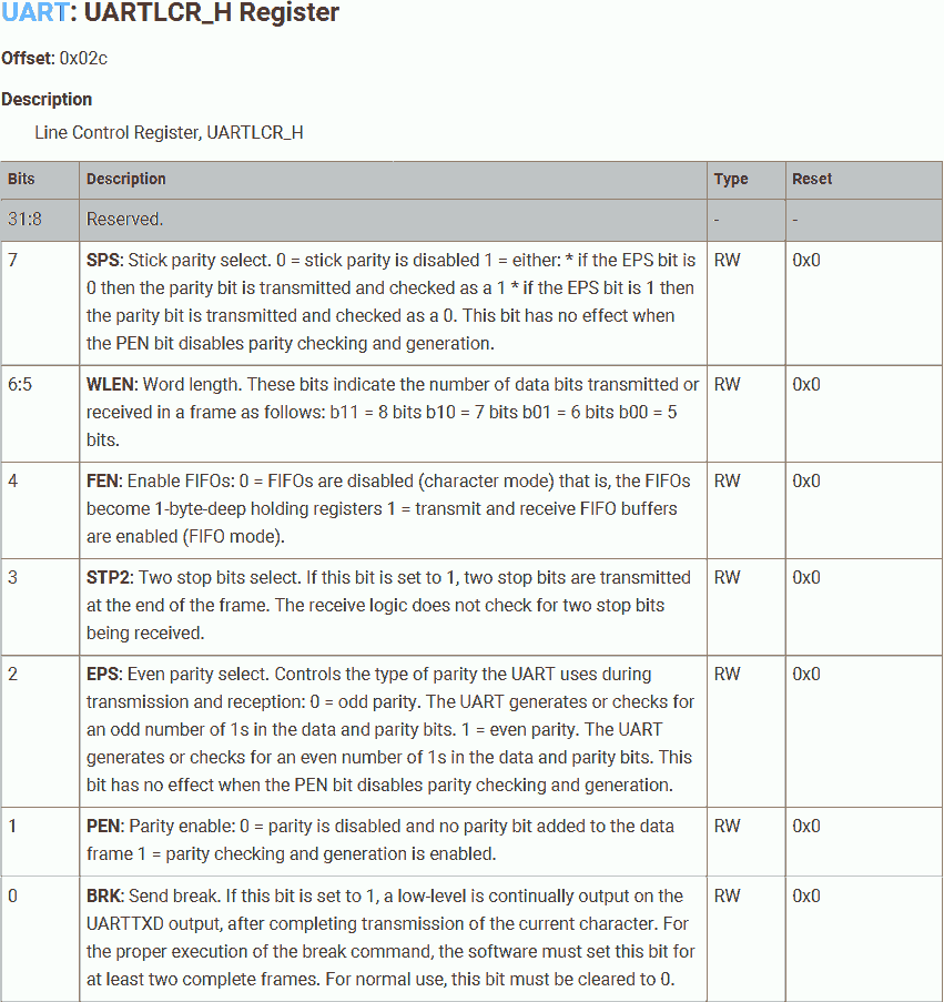
#define reg_uart_uartlcr_h(n)		(0x4003402c + 0x4000 * n)
#define reg_uart_uartlcr_h_sps		7
#define reg_uart_uartlcr_h_wlen		5
#define reg_uart_uartlcr_h_fen		4
#define reg_uart_uartlcr_h_stp2		3
#define reg_uart_uartlcr_h_eps		2
#define reg_uart_uartlcr_h_pen		1
#define reg_uart_uartlcr_h_brk		0
	reg(reg_uart_uartlcr_h(0))
		= ((8-5)<<reg_uart_uartlcr_h_wlen)
		| (1<<reg_uart_uartlcr_h_fen)
		| (1<<reg_uart_uartlcr_h_stp2);
Then, the line control, which means the UART frame format. We will use:
- 8-bit data length.
- Using the Tx/Rx FIFO. (32 words depth in both direction)
- 2 stop bits. Note this only affects the transmitter part. It provides a more reliable signal because it gives longer stop bit length to compensate for clock error.
UART Configuration - Enable
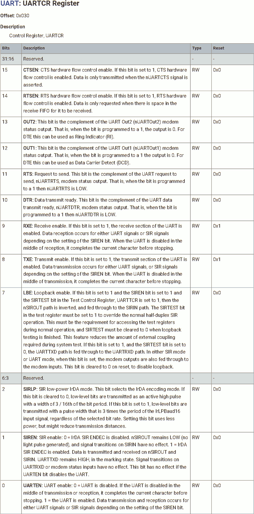
#define reg_uart_uartcr(n)		(0x40034030 + 0x4000 * n)
#define reg_uart_uartcr_ctsen			15
#define reg_uart_uartcr_rtsen			14
#define reg_uart_uartcr_out2			13
#define reg_uart_uartcr_out1			12
#define reg_uart_uartcr_rts			11
#define reg_uart_uartcr_dtr			10
#define reg_uart_uartcr_rxe			9
#define reg_uart_uartcr_txe			8
#define reg_uart_uartcr_lbe			7
#define reg_uart_uartcr_sirlp			2
#define reg_uart_uartcr_siren			1
#define reg_uart_uartcr_uarten		0
	reg(reg_uart_uartcr(0))
		= (1<<reg_uart_uartcr_rxe)
		| (1<<reg_uart_uartcr_txe)
		| (1<<reg_uart_uartcr_uarten);
At the end, enable UART, including both Tx (transmitter) and Rx (receiver).
The UART must be fully configured before enable.
Receiving Data from PC
In a dead loop:
Receiving from UART
#define reg_uart_uartdr(n)		(0x40034000 + 0x4000 * n)
#define reg_uart_uartdr_oe		11 // Overrun
#define reg_uart_uartdr_be		10 // Break error
#define reg_uart_uartdr_pe		9 // Parity error
#define reg_uart_uartdr_fe		8 // Framing error
#define reg_uart_uartdr_data		0 // Tx/Rx data (FIFO)

#define reg_uart_uartfr(n)		(0x40034018 + 0x4000 * n)
#define reg_uart_uartfr_ri		8 // Ring indicator
#define reg_uart_uartfr_txfe		7 // Tx fifo empty
#define reg_uart_uartfr_rxff		6 // Rx fifo full
#define reg_uart_uartfr_txff		5 // Tx fifo full
#define reg_uart_uartfr_rxfe		4 // Rx fifo empty
#define reg_uart_uartfr_busy		3
#define reg_uart_uartfr_dcd		2 // Data carrier detect
#define reg_uart_uartfr_dsr		1 // Data set ready
#define reg_uart_uartfr_cts		0 // Clear to send
	for(;;) {
		while ( reg(reg_uart_uartfr(0)) & (<<reg_uart_uartfr_rxfe) );
		char received = reg(reg_uart_uartdr(0));
First, polling the UART flag register for any incoming data. Is the Rx FIFO empty?
If false, read from the Rx FIFO.
Send to Core 1
#define reg_sio_fifo_st			0xd0000050
#define reg_sio_fifo_st_roe		3		// Read on empty
#define reg_sio_fifo_st_wof		2		// Write on full
#define reg_sio_fifo_st_rdy		1		// Ready to write (not full)
#define reg_sio_fifo_st_vld		0		// Valid to read (not empty)
#define reg_sio_fifo_wr			0xd0000054
		while (!( reg(reg_sio_fifo_st) & (1<<reg_sio_fifo_st_rdy) ));
		reg(reg_sio_fifo_wr) = received;
	}
}
Next, polling the inter-processor mailbox status register. Is the mailbox ready for new data (not full)?
If true, write the received data into the inter-processor mailbox.
C Language File - Program on Core 1
Now, let's define the program running on core 1:
void c1_reset() __attribute__((section(".c1_text"))) __attribute__((naked));

void c1_reset() {
	(boot3_clearInterprocessorMailboxRx + 1)();

	for(;;) {
Define the entry point for core 1, function c1_reset. Similar to c0_reset, make it naked, place it in section .c1_text.
At the beginning of this function, call boot3_clearInterprocessorMailboxRx to clear the inter-processor mailbox.
Create a dead loop to perform the following tasks:
Receiving Data from Core 0
#define reg_sio_fifo_rd 0xd0000058
		while (!( reg(reg_sio_fifo_st) & (1<<reg_sio_fifo_st_vld) ));
		char received = reg(reg_sio_fifo_rd);
Polling the inter-processor mailbox status register. Is the mailbox valid for reading (not empty)?
If true, read the data from the inter-processor mailbox.
Print the First Message
Before we echo the received data to PC via UART, we want to print a message.
__attribute__((section(".c1_data"))) const static char input[] = "Received character is: ";
We will define a string that is:
__attribute__((section(".c1_data")))- Place this string in section.c1_data, that is in the same SRAM bank as the program running on core 1 (.c1_text), to prevent any structural hazard (occured if we place it in SRAM banks used by core 0) and cache miss (occured if we place it in flash).const- We are not gonna modify this string. This is a hint to the compiler, in other words, the compiler will alert us if we tend to modify it. The compiler will generate the same binary code with or without this keyword.static- Do not place this variable in the local frame (in stack).
		for(const char* ptr = input; *ptr; ptr++) {
			while ( reg(reg_uart_uartfr(0)) & (11<<reg_uart_uartfr_txff) );
			reg(reg_uart_uartdr(0)) = *ptr;
		}
To print this string, we will use a for-loop:
- Create a pointer to point to this string. In C, this pointer will point to the first character in this string.
- The for-loop breaks when the pointer points to zero. In C, a string ends with a null-terminator, which is represented by a zero.
- In each iteration, the pointer is indexed by 1 character (1 byte).
In the for-loop, before sending each character, polling the UART flag register to check the FIFO. Wait if Tx FIFO full.
Once free (Tx FIFO no longer full), send the character by writing it to the UART data register.
Echo the Received Data
		while (!( reg(reg_uart_uartfr(0)) & (1<<reg_uart_uartfr_txfe) ));
		reg(reg_uart_uartdr(0)) = received;
		reg(reg_uart_uartdr(0)) = '\r';
		reg(reg_uart_uartdr(0)) = '\n';
Then, check the UART. Wait until the Tx FIFO is empty. This gives us up to 32 words of space to write.
Once the Tx FIFO is empty, burst write the received character, followed by \r and \n to start a new line on the PC terminal. 3 words in total.
Print the Second Message and Send the Modified Data
		__attribute__((section(".c1_data"))) const static char output[] = "The next ASCII character is: ";
		for(const char* ptr = input; *ptr; ptr++) {
			while ( reg(reg_uart_uartfr(0)) & (11<<reg_uart_uartfr_txff) );
			reg(reg_uart_uartdr(0)) = *ptr;
		}

		while (!( reg(reg_uart_uartfr(0)) & (1<<reg_uart_uartfr_txfe) ));
		reg(reg_uart_uartdr(0)) = received;
		reg(reg_uart_uartdr(0)) = '\r';
		reg(reg_uart_uartdr(0)) = '\n';
	}
}
Send the second message followed by the modified (+1 to its ASCII code) data.
Note the message string const char output[] is longer than the Tx FIFO size. However, we checked the FIFO status before sending any character to prevent the FIFO overrun.
See the Result
Connect the Pico board to a USB-UART-TTL adapter, use GPIO0 for Tx and GPIO1 for Rx.
Next, connect the adapter to a PC, and open a serial terminal. In this example, I use Putty in Serial mode. Set it to 9600 BAUD.
Type a random character on the keyboard, which sends that character to the RP2040 MCU via UART. For example, type the key '1', whose ASCII code is 0x31.
The RP2040 replies the message with the character we sent ('1') and its next character('2'), as shown in the screenshot.
Note that, core 0 or core 1 may start / enter the main program before the other one. In a short period immediately after the MCU boot (in most case, only last few milliseconds), the MCU will not response to our input. Either core 0 has not set up the UART, or core 1 is still cleaning the mailbox.