Compare RP2040 Executable Memory Regions and Load Program From Flash into SRAM
Compare RP2040 executable memory regions (flash XIP space, striped SRAM and banked SRAM). Discuss memory strategies, data hazard and structural hazard. Load program from flash into SRAM then execute from SRAM.
Paspberry Pi Pico, RP2040, ARM, Cortex M0+, Assembly, Baremetal, Memory, Memory structural hazard, Linker script, Virtual memory address, Load memory address, MCU
--by Captdam @ Mar 12, 2026Index
This article is intended for developers who are familiar with 8-bit MCUs and use Assembly and C language to develop bare metal applications, but new to 32-bit RP2040 and ARM Cortex-M0+.
Since we are creating bare metal applications, we will be directly writing to and reading from the MCU control registers. No library is used.
We will rely on the documents heavily. It includes all information we need about the MCU control registers.
Because of the RP2040 document updates, and for some reason they decided to redirect my links to the old document to the new document, I decided to create a copy of the current version (2025-02-20) on my server. You may obtain this document from the official link here (as 2026-02-10).
This article is based on my previous article: Switch RP2040 Clock Source in Baremetal: ROSC, XOSC and PLL, you may want to check it first.
Difference Between Memory Regions
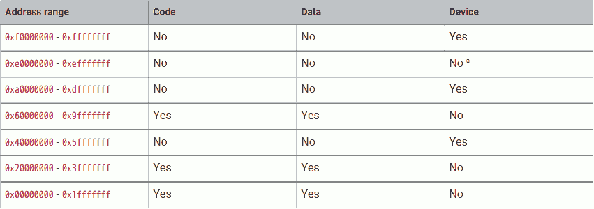
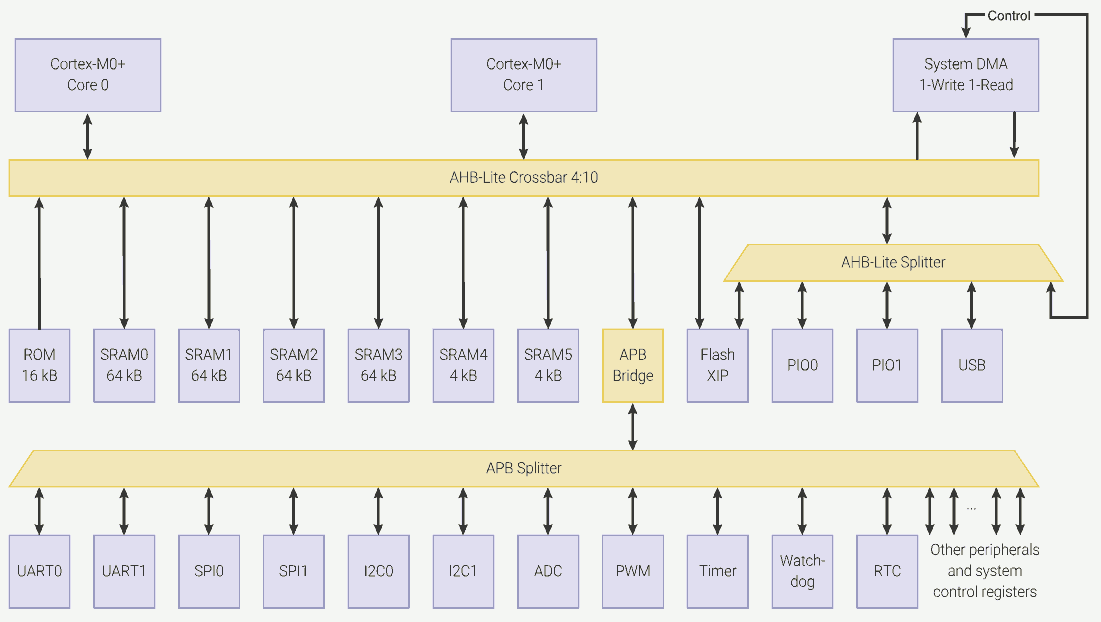
The ARM Cortex M0+ CPU (used in RP2040) is a Von Neumann architecture machine, meaning it has one universal memory space for program, data and device (control registers).
This table shows that different regions in the memory space are for different purposes. Among them, address 0x00000000 to 0x3FFFFFFF and address 0x60000000 to 0x9FFFFFFF can be used for the program.
RP2040 divides these executable memory regions into smaller segments:
- 0x00000000 - 0x00FFFFFF - Boot ROM. 16kiB size. Cannot be used to store user programs. But allows execution from it at boot-up and for some util functions.
- 0x10000000 - 0x1FFFFFFF - (Mapped) external flash via XIP. 16MiB max (24-bit address). Different cache strategies are allowed using different base addresses.
- 0x20000000 - 0x2FFFFFFF - SRAM. 256kiB + 8kiB in size. Different access patterns are allowed using different base addresses.
Boot ROM

The boot ROM is 16kiB in size and it is at the beginning of the RP2040 memory space. Boot ROM is executed at power-up, serving as the first stage bootloader.
Boot ROM is factory-burned and cannot be modified. Hence, we are not allowed to write the boot ROM for our program (user program). Writing to this region will have no effect. However, the Boot ROM provides some util function that can be used in user programs.
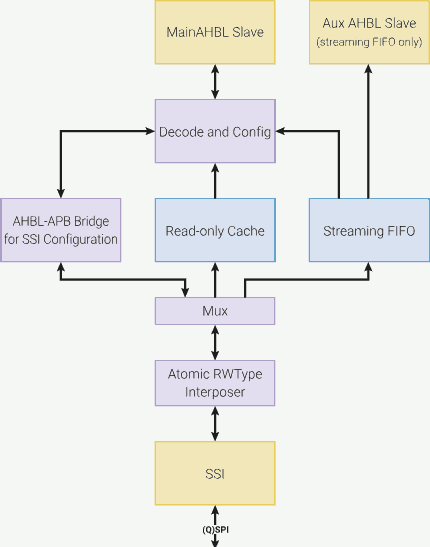
(Mapped) Flash Memory
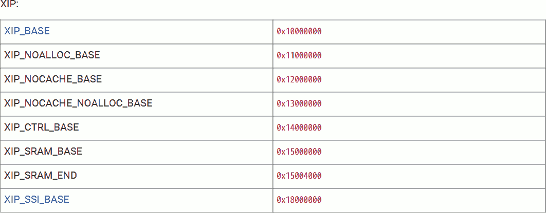
The external flash memory is not directly connected to the RP2040 memory space. However, RP2040 provides XIP in SSI to cache the external flash memory into the XIP memory region. This makes the external flash memory logically a part of the RP2040 internal memory.
The maximum flash size is 16MiB, or 0xFFFFFF bytes, which translates to a 24-bit address. The flash is mirrored four times with different cache strategies:
- 0x10000000 - 0x10FFFFFF - cacheable, allocating. Reading will check cache first. If miss, cache will be updated.
- 0x11000000 - 0x11FFFFFF - cacheable, non-allocating. Reading will check cache first. If miss, read from flash but don't update cahce.
- 0x12000000 - 0x12FFFFFF - non-cacheable, allocating. Reading will not check cache. Always read from flash and update cache.
- 0x13000000 - 0x13FFFFFF - non-cacheable, non-allocating. Bypass cache. Always read from flash, don't update cache.
The XIP cache is 2-way set-associative and its size is 16 kiB. Making it favored in a dual-core sequential execution or near-location read scenario. Hit is 1 cycle.
If the cache misses, the XIP must read the required data from flash. This causes stall.
The Pico on-board flash is 2MiB in size.
SRAM
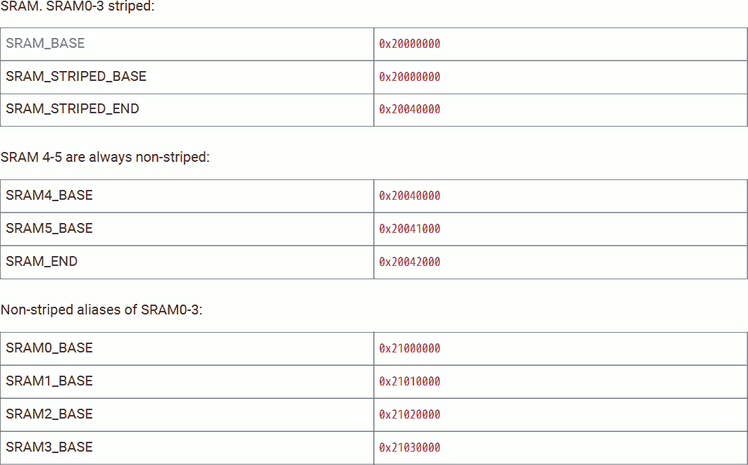
RP2040 provides 264 kiB of SRAM memory in 6 banks. SRAM banks 0 to 3 are 64 kiB each, banks 4 and 5 are 64 kiB. Reading or writing are 1 cycle.
The 4 64k memory banks can be grouped into a 256 kiB striped block. The Striped memory is mapped at address 0x20000000 - 0x2003FFFF. Among them, 0x20000000 is mapped to word 0 of SRAM bank 0, 0x20000004 is mapped to word 0 of bank 1, 0x20000010 is mapped to word 1 of bank 0, and so on.
Striped SRAM makes the highest random access performance. When a core is accessing a specific SRAM bank, there is only a 1/4 chance that the second core is accessing the same SRAM bank. Hence, 25% chance of structural hazard.
The 2 4k SRAM banks can not be striped. SRAM bank 4 is mapped at address 0x20040000 - 0x20040FFF, SRAM bank 5 is mapped at address 0x20041000 - 0x20041FFF.
We can treat the striped four 64k banks and two 4k banks to a universal 264 kiB memory chunk.
If we do not want to use striped SRAM banks 0 to 3, we can access them through address 0x21000000 - 0x2103FFFF. Among them, bank 0 on 0x21000000 - 0x2100FFFF, bank 1 on 0x21010000 - 0x2101FFFF, and so on.
Unstriped SRAM is best when we dedicate SRAM banks to a core. If we can make sure that a bank dedicated to one core will never be accessed by another core (or by DMA), there will be no structural hazard.
We can not treat the two 4k banks and the unstriped four 64k to a universal memory chunk, because they are not continued, address 0x20042000 - 0x20FFFFF is void. However, we can treat the unstriped four 64k to a universal 256 kiB memory chunk.
Other Memories
RP2040 comes with 2 buffers that can be used for data and program if the buffer is not used for its intended purpose:
- XIP cache - 16kiB at 0x15000000
- USB DPRAM - 4kiB at 0x50100000 (Yes, it is executable)
Stall
Cache Miss
The CPU is running faster than external devices. To prevent the external devices from slowing down the CPU, data from external devices must be cached into a small but fast (same speed as CPU or just little slower than the CPU) memory. When the CPU reads data from the external device, it does not read and wait for the external devices; instead, it reads the cache. If the required data is in the cache, the CPU reads it with zero delay (or a few cycles of delay). If the data is not cached, then the CPU stalls, until that data is loaded into the cache. Cache miss is harmless except for delay.
This terminology is used in modern PC CPUs and memory. The CPU (running at some GHz) is tens or hundreds of times faster than the memory (running at some hundreds MHz, note the data transfer speed is different from the memory clock speed). Hence, the CPU comes with an internal data cache and an internal instruction cache. In some cases, there will be multiple stages of CPU caches (L1, L2, L3 caches).
The CPU used in RP2040 does not have cache. SRAM is clocked at the same speed as the CPU, accessing is 1 cycle. However, the external flash device which stores the program is cached (XIP cache). When we execute a program in the flash memory space, the CPU reads the instruction (or program data) at a specific address in the XIP memory space. The XIP hardware will first check if the required instruction (or data) is cached. If hit, the instruction (or data) is returned immediately. If not, the CPU stalls, until the XIP hardware reads the required instruction (or data) from the external flash device into the XIP cache.
The XIP cache is 2-way and 16 kiB in size.
Structural Hazard
Structural hazard occurs when a resource is accessed by multiple devices, but the resource can only respond to one device at a time. Hence, some of the devices must temporarily stall (waiting). Structural hazard is harmless except for delay.
The CPUs used in RP2040 have no cache. When executing an instruction at a specific address, the instruction must be read from that address at the time of execution. Similarly, when reading or writing data at a specific location (either a general data or a control register value), the data must be read or written to or from that address at the time of execution.
As the figure shows, the 4:10 AHB-Lite crossbar is used to connect the CPUs and DMA to the memory spaces. At the same time, each upstream (for example, CPU 0 - AHB-Lite crossbar) and downstream (for example, SRAM 0 - AHB-Lite crossbar) can have at maximum one read or write operation.
Therefore, memory read / write instructions like ldr and str require 2 cycles to complete. The first cycle is used to read the instruction; the second cycle is used to read or write the data.
Furthermore, if two CPUs (or one CPU and the DMA) are trying to access the same downstream memory or device, one must stall until the other one finishes the access.
The access priority can be configured for reach of the 4 upstreams (CPU 0, CPU 1, DMA write and DMA read). If two upstreams with the same priority access the same downstream memory or device at the same time, priority is given in a round-robin fashion.
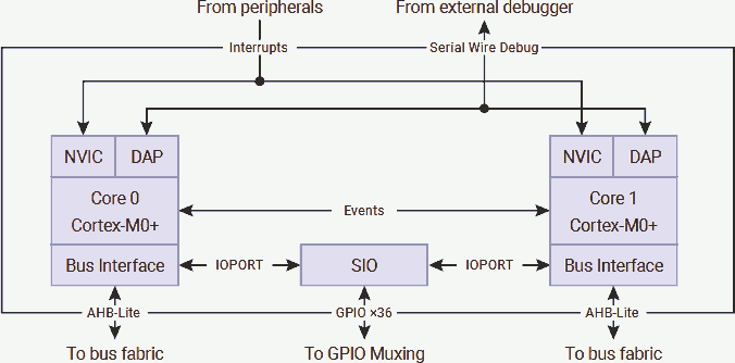
On the other hand, reading from or writing to SIO only consumes 1 CPU cycle, because the SIO is directly connected to the CPU without routing it to the AHB-Lite crossbar. That means, reading the instruction from memory via AHB-Lite crossbar and accessing the SIO can occur in the same cycle.
If two CPUs are written to the same SIO (GPIO output only) at the same time, the write from CPU 0 applied first, then immediately be overwritten by CPU 1. In other words, only the output from CPU 1 takes effect.
Memory Strategy
In this example, assume we are creating a timing-critical dual-core application that we would like to avoid any chance of cache miss and structural hazard. That means:
- To avoid cache miss: We will place the program in SRAM only.
- To avoid structural hazard: We will make each SRAM banks dedicated for one core access.
Following pattern shows what I will use in this example:
- SRAM bank 0 and 1: Dedicated data memory for CPU 0. (128kiB)
- SRAM bank 2 and 3: Dedicated data memory for CPU 1. (128kiB)
- SRAM bank 4: Vector, read-only data (constants), stack and program instruction for CPU 0. (4kiB)
- SRAM bank 5: Vector, read-only data (constants), stack and program instruction for CPU 1. (4kiB)
- Flash: Data or program not immediately in use. Can be loaded into SRAM later when about to required.
Since reading from or writing to SRAM always takes 2 cycles, it is OK to place data of one core in the same SRAM bank as its program.
In most cases, the program is small but the data is large. Therefore, I decided to use the small SRAM banks for programs and large SRAM banks for data. Furthermore, I do not like recursion; hence, the stack will not be very large. It is absolutely fine to use the larger SRAM banks for the program or place the program and stack in different banks.
I will not use the striped memory. It is useful only when the programmer does not use a dedicated memory bank for each upstream. It provides no guarantee but unclear timing.
Dual-core Application Start From USB
Project file for USB boot can be found here.
3rd stage Bootloader
First, we will create an assembly code program called boot3 (bootloader 3). This program will launch core 1 with core 1's program and then start core 0 with core 0's program. Save this file as boot3.s:
.cpu cortex-m0plus
.thumb
.align 2
.thumb_func

.section .boot, "ax"

.global boot3
boot3:
	@ Start core 1 main program
	ldr	r7, =c1_vector
	ldr	r6, =0xd0000050		@ SIO_FIFO_ST
	mov	r0, #1
	str	r0, [r6, #0x04]		@ SIO_FIFO_WR = 1
	str	r7, [r6, #0x04]		@ SIO_FIFO_WR = c1_vector
	ldr	r0, [r7, #0x00]
	str	r0, [r6, #0x04]		@ SIO_FIFO_WR = c1_vector[0] = SP
	ldr	r0, [r7, #0x04]
	str	r0, [r6, #0x04]		@ SIO_FIFO_WR = c1_vector[1] = c0_reset
	sev

	@ Enter core 0 main program
	ldr	r7, =c0_vector
	ldr	r0, [r7, #0x00]		@ c1_vector[0] = SP
	mov	sp, r0
	ldr	r0, [r7, #0x04]		@ c1_vector[1] = c1_reset
	bx	r0

.global boot3_clearInterprocessorMailboxRx
boot3_clearInterprocessorMailboxRx:
	push	{r0, r1}
	ldr	r1, =0xd0000050		@ SIO_FIFO_ST
1:	ldr	r0, [r1, #0x00]		@ SIO_FIFO_ST
	lsr	r0, #1			@ VLD
	bcc	2f
	ldr	r0, [r1, #0x08]		@ SIO_FIFO_RD
	b	1b
2:	mov	r0, #0b1100
	str	r0, [r1, #0x00]		@ SIO_FIFO_ST
	pop	{r0, r1}
	bx	lr
There is nothing new in the boot3 routine. We had discussed this in previous article that launches core 1.
We do create a subroutine that helps empty the inter-processor mailbox, the boot3_clearInterprocessorMailboxRx. This subroutine reads the mailbox FIFO until the FIFO is no longer valid (which means FIFO empty). This subroutine should be executed at the beginning of core 0 and core 1's most beginning.
Once both cores are running and their mailboxes are cleared, the bootloader is no longer required. Programs can use SRAM banks 0 to 3 and overwrite this bootloader.
Name this section .boot and make it allocatable and executable so the linker can allocate space for them. Also make the two routines global so we can use them in other files.
Program on Core 0
Next, we will create an assembly code program that running on core 0. Save this file as main.s:
Data Dedicated to Core 0
.section .c0_data, "aw"

c0_static0:	.space	3
c0_static1:	.byte	0x15
Create a new section .c0_data for core 0's data:
c0_static0- Reserve 3 bytes for this data. The initial value is undefined (, assembler will fill this with 0).c0_static1- 1-byte long. Initial value is 0x15.
I am not gonna use these variables. I just want to show that data dedicated to core 0 is stored in the same SRAM bank as the program for core 0.
Vector Table for Core 0
.section .c0_vector, "aw"
.global c0_vector
c0_vector:
	.word	0x20041000
	.word	c0_reset + 1
Create a new section .c0_vector for core 0's vector table:
- The first vector is the initial SP. Set it to the top of SRAM bank 4.
- The second vector is core 0's entry point. Set it to
c0_reset. Furthermore, Thumb requires the LSB of instruction address to be set; hence, add 1.
Although the vector table should contain 48 32-bit vectors, we are not using any interrupt in this example, we can omit them.
Program for Core 0
.section .c0_text, "awx"

.global c0_reset
c0_reset:
	bl	boot3_clearInterprocessorMailboxRx

	ldr	r7, =0x4000f000		@ RESETS_RESET  + 0x3000
	mov	r0, #(1<<5)		@ IO_BANK0
	str	r0, [r7, #0x00]
	ldr	r7, =0x400140cc		@ IO_BANK0_GPIO25_CTRL
	mov	r0, #5			@ SIO
	str	r0, [r7, #0x00]
	ldr	r7, =0xd0000020		@ SIO_GPIO_OE
	ldr	r0, =(1<<25)		@ GPIO25
	str	r0, [r7, #0x00]

	ldr	r0, =c1_static0
	mov	r8, r0
1:
	mov	r0, r8
@	ldm	r0, {r0, r1, r2, r3, r4, r5, r6, r7}	@ Structural hazard test
	b	1b
Create a new section .c0_text for core 0's program:
There is only one routine called c0_reset. We will:
- Call
boot3_clearInterprocessorMailboxRxdefined inboot3to empty the mailbox. - Configure GPIO to allow output.
- Structural hazard test. This optional section is used to cause structural hazard in core 1. We will comment this section out for now.
Program on Core 1
Then, create a C language program that running on core 1. Save this file as main.c:
Program for Core 1
#include <stdint.h>

extern void boot3_clearInterprocessorMailboxRx();

void c1_reset() __attribute__((section (".c1_text"))) __attribute__((naked));
void c1_reset() {
	boot3_clearInterprocessorMailboxRx();
	for (;;) {
		*(uint32_t volatile * const)(0xd000001c) = (1<<25); // GPIO XOR
	}
}
Declear external function boot3_clearInterprocessorMailboxRx. This tells the compiler that the function boot3_clearInterprocessorMailboxRx is external. Therefore, when compile, the compiler won't panic when it cannot find this function. (Wait until linking)
Define main function for core 1 c1_reset, using attributes:
section (".c1_text")- Place this function in section.c1_textinstead of the default program (instruction text) section.text.naked- This is the main function, it will never return; hence, there is no need to preserve its calling stack. By default, the link registerlrand other general purpose registers used in this function should be pushed into stack to preserve its value, because the caller expecting no change in these registers. Making the main functionnakedcan save some stack space.
In this function, we will:
- Call
boot3_clearInterprocessorMailboxRxdefined inboot3to empty the mailbox. - In a dead loop, flip the GPIO output.
Vector Table for Core 1
uint32_t c1_vector[48] __attribute__ ((section(".c1_vector"))) = {
	0x20042000,
	(uint32_t)c1_reset
};
Define the vector table, its section name is .c1_vector. In this vector table:
- The first vector is the initial SP. Set it to the top of SRAM bank 5.
- The second vector is core 1's entry point. Set it to
c1_reset. In C language, the compiler automatically set the address LSB.
We are not using any interrupt in this example, leave these vectors undefined.
Data Dedicated to Core 1
__attribute__((section (".c1_data"))) volatile uint32_t c1_static0 = 5;
Create a new section .c1_data for core 1's data:
Define a variable c1_static0, that:
- This variable is dedicated to core 1. So, let's put it in section
.c1_data. - Its initial value is 5.
- Make it
volatile, this prevents the compiler from optimizing it into a register-save variable.
I am not gonna use these variables in core 1. I just want to show that data dedicated to core 1 is stored in the same SRAM bank as the program for core 1.
Link and Compile
Now, create a linker script main.ld:
MEMORY {
	SRAM(rwx) : ORIGIN = 0x20000000, LENGTH = 256k
	SRAM_4(rwx) : ORIGIN = 0x20040000, LENGTH = 4k
	SRAM_5(rwx) : ORIGIN = 0x20041000, LENGTH = 4k
	SRAM_0(rwx) : ORIGIN = 0x21000000, LENGTH = 64k
	SRAM_1(rwx) : ORIGIN = 0x21010000, LENGTH = 64k
	SRAM_2(rwx) : ORIGIN = 0x21020000, LENGTH = 64k
	SRAM_3(rwx) : ORIGIN = 0x21030000, LENGTH = 64k
}

ENTRY(boot3)

SECTIONS {
	.text : {
		*(boot3)
		*(boot3_clearInterprocessorMailboxRx)
	} > SRAM

	.core0 : {
		. = ALIGN (256);
		*(.c0_vector)
		*(.c0_data)
		*(.c0_text)
	} > SRAM_4

	.core1 : {
		. = ALIGN (256);
		*(.c1_vector)
		*(.c1_data)
		*(.c1_text)
	} > SRAM_5
}
First, provide the address of each memory banks.
Place our 3rd stage bootloader boot3 and boot3_clearInterprocessorMailboxRx in SRAM (striped memory banks). Set the entry point to boot3.
For USB boot, the entry point must be the beginning of striped memory at 0x20000000 (Thumb 0x20000001). Furturemore, the section name must be .text.
Place core 0's vector table .c0_vector, data .c0_data, program .c0_text in SRAM bank 4. Vector table first.
Place core 1's vector table .c1_vector, data .c1_data, program .c1_text in SRAM bank 5.
It is redundant to place . = ALIGN (256) before vector tables, because the beginning of each bank is 4k aligned.
Next, compile this project:
arm-none-eabi-as --warn --fatal-warnings -g boot3.s -o boot3.o
arm-none-eabi-objdump --disassembler-options=force-thumb -Dxs boot3.o > boot3.s.list

arm-none-eabi-as --warn --fatal-warnings -g main.s -o main.s.o
arm-none-eabi-objdump --disassembler-options=force-thumb -Dxs main.s.o > main.s.list

arm-none-eabi-gcc -mcpu=cortex-m0plus -c -O3 main.c -o main.c.o
arm-none-eabi-objdump --disassembler-options=force-thumb -Dxs main.c.o > main.c.list

arm-none-eabi-ld -nostdlib -nostartfiles -T main.ld boot3.o main.s.o main.c.o -o main.elf
arm-none-eabi-objdump --disassembler-options=force-thumb -dxs main.elf > main.list
pico-elf2uf2 main.elf main.uf2
Verify Output
Now, we can verify the out using the disassembled code main.list:
boot
Disassembly of section .boot:

20000000 <boot3>:
20000000:	4f0c      	ldr	r7, [pc, #48]	; (20000034 <boot3_clearInterprocessorMailboxRx+0x16>)
20000002:	4e0d      	ldr	r6, [pc, #52]	; (20000038 <boot3_clearInterprocessorMailboxRx+0x1a>)
20000004:	2001      	movs	r0, #1
20000006:	6070      	str	r0, [r6, #4]
20000008:	6077      	str	r7, [r6, #4]
2000000a:	6838      	ldr	r0, [r7, #0]
2000000c:	6070      	str	r0, [r6, #4]
2000000e:	6878      	ldr	r0, [r7, #4]
20000010:	6070      	str	r0, [r6, #4]
20000012:	bf40      	sev
20000014:	4f09      	ldr	r7, [pc, #36]	; (2000003c <boot3_clearInterprocessorMailboxRx+0x1e>)
20000016:	6838      	ldr	r0, [r7, #0]
20000018:	4685      	mov	sp, r0
2000001a:	6878      	ldr	r0, [r7, #4]
2000001c:	4700      	bx	r0

2000001e <boot3_clearInterprocessorMailboxRx>:
2000001e:	b403      	push	{r0, r1}
20000020:	4905      	ldr	r1, [pc, #20]	; (20000038 <boot3_clearInterprocessorMailboxRx+0x1a>)
20000022:	6808      	ldr	r0, [r1, #0]
20000024:	0840      	lsrs	r0, r0, #1
20000026:	d301      	bcc.n	2000002c <boot3_clearInterprocessorMailboxRx+0xe>
20000028:	6888      	ldr	r0, [r1, #8]
2000002a:	e7fa      	b.n	20000022 <boot3_clearInterprocessorMailboxRx+0x4>
2000002c:	200c      	movs	r0, #12
2000002e:	6008      	str	r0, [r1, #0]
20000030:	bc03      	pop	{r0, r1}
20000032:	4770      	bx	lr

20000034:	20041000 	.word	0x20041000
20000038:	d0000050 	.word	0xd0000050
2000003c:	20040000 	.word	0x20040000
Routine boot3 is placed at the beginning of the striped SRAM at address 0x20000000. This routine will be executed at boot.
Routine boot3_clearInterprocessorMailboxRx is placed immediately after boot3, at address 0x2000001e, in striped SRAM.
Followed by constants used in the assembly code, including:
.word 0x20041000 @ 20000034- Vector table address for core 1..word 0x20040000 @ 2000003C- Vector table address for core 0.
core0
Disassembly of section .core0:

20040000 <c0_vector>:
20040000:	20041000 	.word	0x20041000
20040004:	2004000d 	.word	0x2004000d

20040008 <c0_static0>:
20040008:	0000      	.short	0x0000
	...

2004000b <c0_static1>:
2004000b:	15          	.byte	0x15

2004000c <c0_reset>:
2004000c:	f7c0 f807 	bl	2000001e <boot3_clearInterprocessorMailboxRx>
20040010:	4f06      	ldr	r7, [pc, #24]	; (2004002c <c0_reset+0x20>)
20040012:	2020      	movs	r0, #32
20040014:	6038      	str	r0, [r7, #0]
20040016:	4f06      	ldr	r7, [pc, #24]	; (20040030 <c0_reset+0x24>)
20040018:	2005      	movs	r0, #5
2004001a:	6038      	str	r0, [r7, #0]
2004001c:	4f05      	ldr	r7, [pc, #20]	; (20040034 <c0_reset+0x28>)
2004001e:	4806      	ldr	r0, [pc, #24]	; (20040038 <c0_reset+0x2c>)
20040020:	6038      	str	r0, [r7, #0]
20040022:	4806      	ldr	r0, [pc, #24]	; (2004003c <c0_reset+0x30>)
20040024:	4680      	mov	r8, r0
20040026:	4640      	mov	r0, r8
20040028:	e7fd      	b.n	20040026 <c0_reset+0x1a>
2004002a:	0000      	.short	0x0000

2004002c:	4000f000 	.word	0x4000f000
20040030:	400140cc 	.word	0x400140cc
20040034:	d0000020 	.word	0xd0000020
20040038:	02000000 	.word	0x02000000
2004003c:	200410c0 	.word	0x200410c0
Vector table for core 0 c0_vector is placed at the beginning of the SRAM bank 4 at address 0x20040000. It is 256-byte aligned.
Data dedicated to core 0 c0_static0 and c0_static1 is placed immediately after c0_vector, at address 0x20040008, in SRAM bank 4.
c0_static0 and c0_static1 are byte data. No align required.
Program for core 0 c0_reset is placed immediately after c0_static1, at address 0x2004000c, in SRAM bank 4.
Followed by constants used in the assembly code.
core1
Disassembly of section .core1:

20041000 <c1_vector>:
20041000:	20042000 200410c5 00000000 00000000     . . ... ........
	...

200410c0 <c1_static0>:
200410c0:	00000005                                ....

200410c4 <c1_reset>:
200410c4:	f7be ffab 	bl	2000001e <boot3_clearInterprocessorMailboxRx>
200410c8:	2380      	movs	r3, #128	; 0x80
200410ca:	4a02      	ldr	r2, [pc, #8]	; (200410d4 <c1_reset+0x10>)
200410cc:	049b      	lsls	r3, r3, #18
200410ce:	6013      	str	r3, [r2, #0]
200410d0:	6013      	str	r3, [r2, #0]
200410d2:	e7fc      	b.n	200410ce <c1_reset+0xa>
200410d4:	d000001c 	.word	0xd000001c
Vector table for core 1 c1_vector is placed at the beginning of the SRAM bank 5 at address 0x20041000. It is 256-byte aligned.
Data dedicated to core 1 c1_static0 is placed immediately after c1_vector, at address 0x200410c0, in SRAM bank 5.
Program for core 1 c1_reset is placed immediately after c1_static0, at address 0x200410c4, in SRAM bank 5.
For some reasons, the compiler decided to flip the output twice in the loop. We can see 2 lines of str r3, [r2, #0].
Followed by constants used in the assembly code.
Measure the Output
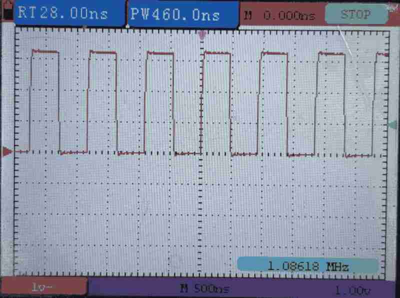
Download the uf2 file. Then, use an oscilloscope to measure the output waveform.
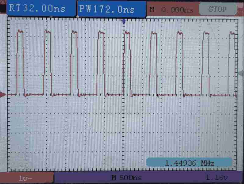
By default, ROSC is used as the system clock source. Which is running at 5.8MHz on my chip.
Writing SIO consumes 1 cycles, branch consumes 2 cycles. Therefore, we are seeing the output waveform at 5.8MHz / 4 = 1.45MHz with 1/4 duty.
Structural Hazard in Effect
To verify that accessing the same memory bank from two cores at the same time could stall the process, we will add a dead loop in core 0's program. In this dead loop, we will try to read from the SRAM bank storing core 1's instruction. In this case, the SRAM bank has to serve both instruction read from core 1 and data read from core 0 at the same time.
	ldr	r0, =c1_static0
	mov	r8, r0
1:
	mov	r0, r8
	ldm	r0, {r0, r1, r2, r3, r4, r5, r6, r7}	@ Structural hazard test
	b	1b
We will uncomment this line in c0_reset: ldm r0, {r0, r1, r2, r3, r4, r5, r6, r7}. In this loop, we will:
- Load the address of
c1_static0, which is saved in the same SRAM bank as core 1's program instructions. - Load r0 with that address. (1 cycle)
- Read 8 words using r0 as a pointer, causing structural hazard on the SRAM bank used by core 1. (9 cycles, 8 reads)
- Go to step 2 and repeat. (2 cycles)
That is, in every 12 cycles in core 0, stall core 1 for 8 cycles.
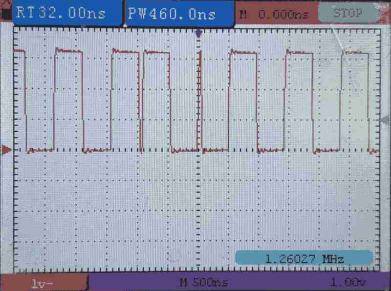
Compile, link, and download the uf2 file. Then, use an oscilloscope to measure the output waveform.
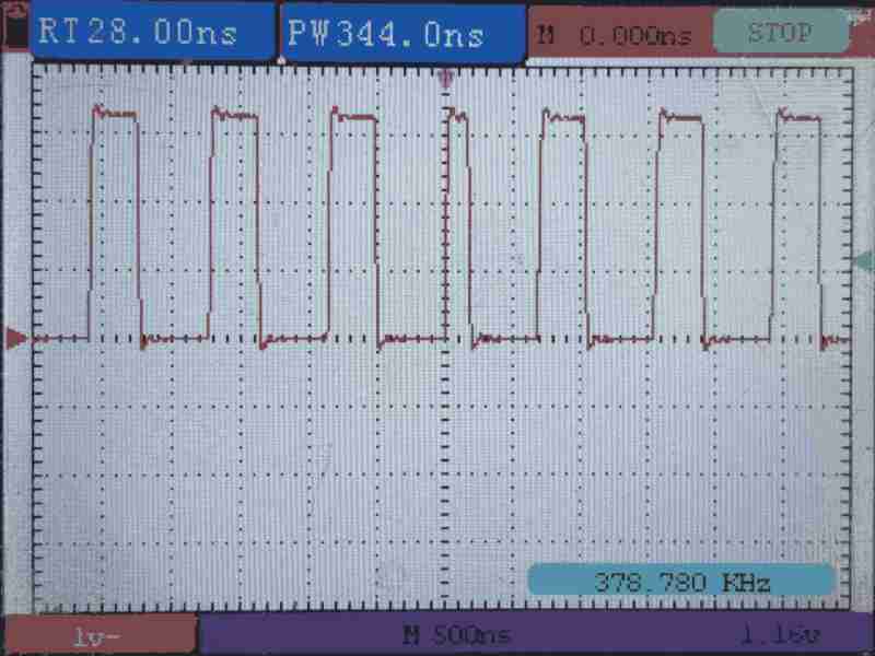
As the scope shows, the frequency lowered, meaning core 1 stalls.
Since the AHB-Lite crossbar access is given in a round-robin fashion, sometimes core 1 will stall core 0 (shows same waveform length as the last figure), sometimes core 0 will stall core 1 (shows longer waveform length).
Dual-core Application Start from Flash
In the previous example, we successfully downloaded the dual-core program into SRAM banks 4 and 5, each bank is dedicated for one core, preventing any stall from structural hazard.
However, once power was lost, the program disappeared. Is there a way that we can store the program into flash, then load the program from flash into SRAM banks at boot time?
On a PC, when we compile a program, the program is not only a bunch of CPU instructions, but also includes information about how to set up the run-time environment and prepare the data, making the program executable. When we execute a program:
- The operating system (OS) started.
- The OS loads the program file from disk into memory.
- The OS reads the program file's "information" section, sets up the run-time environment, places its contents (program and data segments) into the desired address.
- Load PC with the entry point and starting execution.
We will do the similar tasks on RP2040:
- The on-chip bootloader starts the 2nd stage bootloader in striped SRAM. Then, the 2nd stage bootloader configures XIP in SSI. This is similar to starting the OS.
- The 2nd stage bootloader starts our 3rd stage bootloader. The 3rd stage bootloader is saved and executed in flash (XIP) memory space.
- Our 3rd stage bootloader copies the vector tables, data, and program instructions into SRAM banks. Furthermore, the 3rd stage bootloader performs other setups, such as clock source, memory protection, interrupt vector setup, and ect..
- Our 3rd stage bootloader (running on core 0) launches core 1 with core 1's main program, and branches to core 0's main program.
Project file for flash boot can be found here.
3rd stage Bootloader
First, we will create an assembly code program called boot3 (bootloader 3). Similar to the previous example, this program will launch core 1 with core 1's program and then start core 0 with core 0's program. Furturemore, this program will set the system clock to 133MHz PLL and copy the program from the flash memory space into the SRAM banks. Save this file as boot3.s:
Boot section
.cpu cortex-m0plus
.thumb
.align 2
.thumb_func

.section .boot3, "awx"
Place the entire file in .boot3 section and make it allocatable and executable so the linker can allocate space for them.
Vector Table
	.word	0x20041000
	.word	boot3 + 1
As required by the 2nd stage bootloader we used (the SDK 2nd stage bootloader), we have to place the vector table at the beginning. The vector table includes:
- Initial SP used by this program. We will set it to the top of SRAM bank 4.
- Entry point. We will set it to the routine
boot3. Because it is a Thumb instruction routine, set the LSB of its address.
boot3_copyText
boot3_copyText:
	ldrh	r3, [r1, #0]		@ r1 = src, use halfword because insturction is 16-bit wide, code block may not be 4-byte aligned
	strh	r3, [r0, #0]		@ r0 = dest
	add	r1, #2
	add	r0, #2
	cmp	r1, r2			@ r2 = src_top
	bls	boot3_copyText		@ Continue if src less than src_top
	bx	lr
Create a subroutine boot3_copyText. This subroutine is used to copy the program text from flash into SRAM.
This subroutine accepts 3 parameters:
r0- Beginning address of the destination.r1- Beginning address of the source.r2- End (not included) address of the source.r3- Will be clobbed.
This operation can be illustrated by:
for (
	uint16_t* src = program_in_flash_begin, * dest = program_in_sram_begin;
	src < program_in_flash_end;
	src++
) {
	*(dest++) = *(src++);
}
Because the Thumb instruction is 16-bit wide, the length of the content (programs, vector tables and data) is 2-byte aligned. Furthermore, the assembler and compiler will insert padding if the content is not 2-byte aligned. Therefore, we will use half-word read / write instructions ldrh / strh.
This subroutine is used in the bootloader only. Hence, no need to make it global.
There is no harm to place subroutines or data before the main program of our 3rd stage bootloader. The 2nd stage bootloader reads the entry point from the vector table, the entry point can be anywhere.
boot3_clearInterprocessorMailboxRx
.global boot3_clearInterprocessorMailboxRx
boot3_clearInterprocessorMailboxRx:
	push	{r0, r1}
	ldr	r1, =0xd0000050		@ SIO_FIFO_ST
1:	ldr	r0, [r1, #0x00]		@ SIO_FIFO_ST
	lsr	r0, #1			@ VLD
	bcc	2f
	ldr	r0, [r1, #0x08]		@ SIO_FIFO_RD
	b	1b
2:	mov	r0, #0b1100
	str	r0, [r1, #0x00]		@ SIO_FIFO_ST
	pop	{r0, r1}
	bx	lr
Create a subroutine that helps empty the inter-processor mailbox, the boot3_clearInterprocessorMailboxRx. Discussed in previous example.
This subroutine will be used in the main programs (in other files). Hence, make it global for linking.
boot3
.global boot3
boot3:
	@ Start XOSC
	ldr	r7, =0x40024000			@ XOSC_BASE
	ldr	r0, =0x00FABAA0			@ Enable 1-15MHz
	str	r0, [r7, #0x00]			@ XOSC_CTRL
1:	ldr	r0, [r7, #0x04]			@ XOSC_STATUS
	lsr	r0, #32				@ Stable
	bcc	1b

	@ Start PLL
	ldr	r7, =0x4000f000			@ RESETS_RESET  + 0x3000
	ldr	r0, =(1<<12)			@ PLL_SYS
	str	r0, [r7, #0x00]

	ldr	r7, =0x40028000			@ PLL_SYS_BASE
	ldr	r6, =0x40028000 + 0x3000	@ PLL_SYS_CLEAR
	mov	r0, #(1<<0)			@ RefDiv = 1
	str	r0, [r7, #0x00]			@ PLL_SYS_CS
	mov	r0, #63				@ 12MHz * 63 = 756MHz
	str	r0, [r7, #0x08]			@ PLL_SYS_FBDIV_INT
	mov	r0, #((1<<5) | (1<<0))		@ VO and main powerdown
	str	r0, [r6, #0x04]			@ PLL_SYS_CLEAR_PWR
1:	ldr	r0, [r7, #0x00]			@ PLL_SYS_CS
	lsr	r0, r0, #32			@ Lock
	bcc	1b
	ldr	r0, =((6 << 16) | (1 << 12))	@ 756MHz / (6*1) = 126MHz
	str	r0, [r7, #0x0C]			@ PLL_SYS_PRIM
	mov	r0, #(1<<3)			@ PostDiv powerdown
	str	r0, [r6, #0x04]			@ PLL_SYS_CLEAR_PWR

	@ Switch to PLL
	ldr	r7, =0x40008000			@ CLOCKS_BASE
	mov	r0, #((0<<5) | (0<<0))		@ Set Aux src to CLKSRC_PLL_SYS (need wait) and switch Src to CLK_REF (on-the-fly), for safe
	str	r0, [r7, #0x3C]			@ CLOCKS_CLK_SYS_CTRL
	nop
	nop
	mov	r0, #((0<<5) | (1<<0))		@ Keep Aux src but switch Src to CLKSRC_CLK_SYS_AUX (on-the-fly)
	str	r0, [r7, #0x3C]

	@ Copy Code for core 0
	ldr	r0, =_core0_dest
	ldr	r1, =_core0_start
	ldr	r2, =_core0_end
	bl	boot3_copyText

	@ Copy code for core 1
	ldr	r0, =_core1_dest
	ldr	r1, =_core1_start
	ldr	r2, =_core1_end
	bl	boot3_copyText

	@ Start core 1 main program
	ldr	r7, =c1_vector
	ldr	r6, =0xd0000050		@ SIO_FIFO_ST
	mov	r0, #1
	str	r0, [r6, #0x04]		@ SIO_FIFO_WR = 1
	str	r7, [r6, #0x04]		@ SIO_FIFO_WR = c1_vector
	ldr	r0, [r7, #0x00]
	str	r0, [r6, #0x04]		@ SIO_FIFO_WR = c1_vector[0] = SP
	ldr	r0, [r7, #0x04]
	str	r0, [r6, #0x04]		@ SIO_FIFO_WR = c1_vector[1] = c0_reset
	@ Delay core 1 start until core 0 ready

	@ Enter core 0 main program
	ldr	r7, =c0_vector
	ldr	r0, [r7, #0x00]		@ c1_vector[0] = SP
	mov	sp, r0
	ldr	r0, [r7, #0x04]		@ c1_vector[1] = c1_reset
	sev				@ Core 1 start
	bx	r0
Here is waht we will do in our 3rd stage bootloader. We had discussed the detail in previous article, so, I'm not gonna spend too much time explain this. In summary, this performs:
- Start XOSC.
- Start PLL, which requires XOSC as reference clock.
- Switch the system clock source to PLL, allowing the system to run at maximum frequency (133MHz).
- Copy the programs (including instructions, data and vector tables) from flash to SRAM. The address will be resolved at linking time.
- Launch core 1 and start core 0.
Program on Core 0
Next, we will create an assembly code program that running on core 0. In this example, we will let core 0 to flip the GPIO output. Save this file as main.s:
Data Dedicated to Core 0
.section .c0_data, "aw"

c0_static0:	.space	3
c0_static1:	.byte	0x15
Create a new section .c0_data for core 0's data:
c0_static0- Reserve 3 bytes for this data. The initial value is undefined (, assembler will fill this with 0).c0_static1- 1-byte long. Initial value is 0x15.
I am not gonna use these variables. I just want to show that data dedicated to core 0 is stored in the same SRAM bank as the program for core 0.
Vector Table for Core 0
.section .c0_vector, "aw"
.global c0_vector
c0_vector:
	.word	0x20041000
	.word	c0_reset + 1
Create a new section .c0_vector for core 0's vector table:
- The first vector is the initial SP. Set it to the top of SRAM bank 4.
- The second vector is core 0's entry point. Set it to
c0_reset. Furthermore, Thumb requires the LSB of instruction address to be set; hence, add 1.
Although the vector table should contain 48 32-bit vectors, we are not using any interrupt in this example, we can omit them.
Program for Core 0
.section .c0_text, "awx"

.global c0_reset
c0_reset:
	ldr	r0, =(boot3_clearInterprocessorMailboxRx+1)
	blx	r0

	ldr	r1, =0xd000001c		@ GPIO XOR
	ldr	r0, =(1<<25)		@ GPIO25

	ldr	r2, =0x10000000		@ Flash pointer
	ldr	r3, =0x00000004		@ Flash step (must be 4x for word read)
	ldr	r4, =0x100000FF		@ Flash mask

1:	str	r0, [r1, #0]
	ldr	r5, [r2, #0]
	add	r2, r2, r3
	and	r2, r2, r4
	b	1b
Create a new section .c0_text for core 0's program:
There is only one routine called c0_reset. We will:
- Call
boot3_clearInterprocessorMailboxRxdefined inboot3to empty the mailbox. - Load the registers with addresses and values to write.
- In a dead loop, flip the GPIO output and read a dummy data from flash (cache miss test).
Note that in the example, when calling the subroutine boot3_clearInterprocessorMailboxRx, we cannot use the bl boot3_clearInterprocessorMailboxRx instruction because the bl label instruction only supports PC offset of +/- 16MiB. However, the subroutine is saved in flash space at 0x10000000, the program is running in SRAM space at 0x20000000, the offset is 0x10000000, or 256MiB, which is larger than the allowed offset. Therefore, we have to load the subroutine's address in a register (a function pointer), add 1 because of Thumb instruction, then use the blx rx instruction to call that subroutine.
We will discuss the details of the cache miss test in a later chapter in this article.
Program on Core 1
Then, create a C language program that running on core 1. In this example, we will let core 1 to configure the GPIO output. Save this file as main.c:
Program for Core 1
#include <stdint.h>

__attribute__((long_call)) extern void boot3_clearInterprocessorMailboxRx();

void c1_reset() __attribute__((section (".c1_text"))) __attribute__((naked));
void c1_reset() {
	(boot3_clearInterprocessorMailboxRx + 1)();

	*(uint32_t volatile * const)(0x4000f000) = (1<<5);	// RESETS_RESET + 0x3000 <-- IO_BANK0
	*(uint32_t volatile * const)(0x400140cc) = (5);		// IO_BANK0_GPIO25_CTRL <-- SIO
	*(uint32_t volatile * const)(0xd0000020) = (1<<25);	// SIO_GPIO_OE <-- GPIO25

	for(;;);
}
Declear external function boot3_clearInterprocessorMailboxRx. Furturemore, add the long_call attribute to it. This allows the compiler to use the blx rx instruction to call a subroutine that is more than 16 MiB away from the current address. However, this attribute doesn't tell the compiler whether this function uses Thumb or ARM. We have to manually add 1 (for Thumb) to this symbol when we call it. (Wait until linking)
Define main function for core 1 c1_reset, using attributes:
section (".c1_text")- Place this function in section.c1_textinstead of the default program (instruction text) section.text.naked- This is the main function, it will never return; hence, there is no need to preserve its calling stack. By default, the link registerlrand other general purpose registers used in this function should be pushed into stack to preserve its value, because the caller expecting no change in these registers. Making the main functionnakedcan save some stack space.
In this function, we will:
- Call
boot3_clearInterprocessorMailboxRxdefined inboot3to empty the mailbox. - Configure the GPIO output.
Vector Table for Core 1
uint32_t c1_vector[48] __attribute__ ((section(".c1_vector"))) = {
	0x20042000,
	(uint32_t)c1_reset
};
Define the vector table, its section name is .c1_vector. In this vector table:
- The first vector is the initial SP. Set it to the top of SRAM bank 5.
- The second vector is core 1's entry point. Set it to
c1_reset. In C language, the compiler automatically set the address LSB.
We are not using any interrupt in this example, leave these vectors undefined.
Data Dedicated to Core 1
__attribute__((section (".c1_data"))) volatile uint32_t c1_static0 = 5;
Create a new section .c1_data for core 1's data:
Define a variable c1_static0, that:
- This variable is dedicated to core 1. So, let's put it in section
.c0_data. - Its initial value is 5.
- Make it
volatile, this prevents the compiler from optimizing it into a register-save variable.
I am not gonna use these variables in core 1. I just want to show that data dedicated to core 1 is stored in the same SRAM bank as the program for core 1.
Link and Compile
Now, create a linker script main.ld:
MEMORY {
	FLASH(rwx) : ORIGIN = 0x10000000, LENGTH = 2048k
	SRAM(rwx) : ORIGIN = 0x20000000, LENGTH = 256k
	SRAM_4(rwx) : ORIGIN = 0x20040000, LENGTH = 4k
	SRAM_5(rwx) : ORIGIN = 0x20041000, LENGTH = 4k
	SRAM_0(rwx) : ORIGIN = 0x21000000, LENGTH = 64k
	SRAM_1(rwx) : ORIGIN = 0x21010000, LENGTH = 64k
	SRAM_2(rwx) : ORIGIN = 0x21020000, LENGTH = 64k
	SRAM_3(rwx) : ORIGIN = 0x21030000, LENGTH = 64k
}

ENTRY(_boot_start)

SECTIONS {
	.boot : {
		*(.boot2)
		*(.boot3)
	} > FLASH
	_boot_start = ORIGIN(FLASH);
	_boot_end = _boot_start + SIZEOF(.boot);

	.core0 : {
		. = ALIGN (256)
		*(.c0_vector)
		*(.c0_data)
		*(.c0_text)
	} > SRAM_4 AT > FLASH
	_core0_dest = ORIGIN(SRAM_4);
	_core0_start = _boot_end;
	_core0_end = _core0_start + SIZEOF(.core0);

	.core1 : {
		. = ALIGN (256)
		*(.c1_vector)
		*(.c1_data)
		*(.c1_text)
	} > SRAM_5 AT > FLASH
	_core1_dest = ORIGIN(SRAM_5);
	_core1_start = _core0_end;
	_core1_end = _core1_start + SIZEOF(.core1);

	.unspecified : {
		*(.text)
		*(.data)
		*(.bss)
	}
	ASSERT(!(SIZEOF(.unspecified)), "Unspecified text, data, and/or bss section")
}
The linker script used in this example is a little bit complex.
To execute the program in a memory different than store program, we will provide both virtual memory address (VMA) and load memory address (LMA) for the sections using the following syntax:
.section_name : {
	*(.subsection_name)
	*(.subsection_name)
	*(.subsection_name)
	*(symbol_name)
	*(symbol_name)
} > virtual_memory_addr AT > load_memory_addr
That is:
- Use SRAM bank 4 and 5 for VMA. This address is used when resovle a symbol (variables and routines).
- Use flash for LMA. This address is used to store the programs and data.
Furthermore, we need to define the following symbol to indicate the address of programs and data. They are used to copy the programs, vector tables and data from flash into SRAM banks in our 3rd stage bootloader:
_boot_start- Start of the flash memory._boot_end- End of the.bootsection in flash._core0_start- Same as_boot_end. Section.core0(program, vector table and data for core 0) is placed immediately after the.bootsection._core0_end- End of the.core0section in flash._core1_start- Same as_core0_end. Section.core1(program, vector table and data for core 1) is placed immediately after the.core0section._core1_end- End of the.core1section in flash._core0_dest- Virtual address for.core0, which is SRAM bank 4 in our example._core1_dest- Virtual address for.core1, which is SRAM bank 5 in our example.
In our design, the programs, vector tables and data must be assigned to the .boot, .core0 or .core1 section. We defined a special section named .unspecified to include any data, vector table or program that is not assigned one of the mentioned sections. If there is any content in the .unspecified section, the linking fails. This tells us we forgot something.
First, provide the address of each memory banks.
Place the SDK 2nd stage bootloader .boot2 and our 3rd stage bootloader .boot3 (preserve the order) in the flash.
Entry point is not required for flash boot.
Place core 0's vector table c0_vector, data c0_data, program c0_text in the flash but use SRAM bank 4 for virtual address. Vector table first.
Place core 1's vector table c1_vector, data c1_data, program c1_text in the flash but use SRAM bank 5 for virtual address.
It is redundant to place . = ALIGN (256) before vector tables, because the beginning of each bank is 4k aligned. Furturemore, the alignment only applies to the VMA.
Next, compile this project:
arm-none-eabi-as --warn --fatal-warnings -g boot3.s -o boot3.o
arm-none-eabi-objdump --disassembler-options=force-thumb -Dxs boot3.o > boot3.s.list

arm-none-eabi-as --warn --fatal-warnings -g main.s -o main.s.o
arm-none-eabi-objdump --disassembler-options=force-thumb -Dxs main.s.o > main.s.list

arm-none-eabi-gcc -mcpu=cortex-m0plus -c -O3 main.c -o main.c.o
arm-none-eabi-objdump --disassembler-options=force-thumb -Dxs main.c.o > main.c.list

arm-none-eabi-ld -nostdlib -nostartfiles -T main.ld boot3.o main.s.o main.c.o boot2.o -o main.elf
arm-none-eabi-objdump --disassembler-options=force-thumb -dxs main.elf > main.list
pico-elf2uf2 main.elf main.uf2
Verify Output - Virtual address
Now, we can verify the out using the disassembled code main.list. Note the disassembled code shows virtual address:
boot
Disassembly of section .boot:

10000000 <_boot_start>:
10000000:	4b32b500 	.word	0x4b32b500
10000004:	60582021 	.word	0x60582021
10000008:	21026898 	.word	0x21026898
1000000c:	60984388 	.word	0x60984388
10000010:	611860d8 	.word	0x611860d8
10000014:	4b2e6158 	.word	0x4b2e6158
10000018:	60992100 	.word	0x60992100
1000001c:	61592102 	.word	0x61592102
10000020:	22f02101 	.word	0x22f02101
10000024:	492b5099 	.word	0x492b5099
10000028:	21016019 	.word	0x21016019
1000002c:	20356099 	.word	0x20356099
10000030:	f844f000 	.word	0xf844f000
10000034:	42902202 	.word	0x42902202
10000038:	2106d014 	.word	0x2106d014
1000003c:	f0006619 	.word	0xf0006619
10000040:	6e19f834 	.word	0x6e19f834
10000044:	66192101 	.word	0x66192101
10000048:	66182000 	.word	0x66182000
1000004c:	f000661a 	.word	0xf000661a
10000050:	6e19f82c 	.word	0x6e19f82c
10000054:	6e196e19 	.word	0x6e196e19
10000058:	f0002005 	.word	0xf0002005
1000005c:	2101f82f 	.word	0x2101f82f
10000060:	d1f94208 	.word	0xd1f94208
10000064:	60992100 	.word	0x60992100
10000068:	6019491b 	.word	0x6019491b
1000006c:	60592100 	.word	0x60592100
10000070:	481b491a 	.word	0x481b491a
10000074:	21016001 	.word	0x21016001
10000078:	21eb6099 	.word	0x21eb6099
1000007c:	21a06619 	.word	0x21a06619
10000080:	f0006619 	.word	0xf0006619
10000084:	2100f812 	.word	0x2100f812
10000088:	49166099 	.word	0x49166099
1000008c:	60014814 	.word	0x60014814
10000090:	60992101 	.word	0x60992101
10000094:	2800bc01 	.word	0x2800bc01
10000098:	4700d000 	.word	0x4700d000
1000009c:	49134812 	.word	0x49134812
100000a0:	c8036008 	.word	0xc8036008
100000a4:	8808f380 	.word	0x8808f380
100000a8:	b5034708 	.word	0xb5034708
100000ac:	20046a99 	.word	0x20046a99
100000b0:	d0fb4201 	.word	0xd0fb4201
100000b4:	42012001 	.word	0x42012001
100000b8:	bd03d1f8 	.word	0xbd03d1f8
100000bc:	6618b502 	.word	0x6618b502
100000c0:	f7ff6618 	.word	0xf7ff6618
100000c4:	6e18fff2 	.word	0x6e18fff2
100000c8:	bd026e18 	.word	0xbd026e18
100000cc:	40020000 	.word	0x40020000
100000d0:	18000000 	.word	0x18000000
100000d4:	00070000 	.word	0x00070000
100000d8:	005f0300 	.word	0x005f0300
100000dc:	00002221 	.word	0x00002221
100000e0:	180000f4 	.word	0x180000f4
100000e4:	a0002022 	.word	0xa0002022
100000e8:	10000100 	.word	0x10000100
100000ec:	e000ed08 	.word	0xe000ed08
	...
100000fc:	7a4eb274 	.word	0x7a4eb274
10000100:	20041000 	.word	0x20041000
10000104:	1000012d 	.word	0x1000012d

10000108 <boot3_copyText>:
10000108:	880b      	ldrh	r3, [r1, #0]
1000010a:	8003      	strh	r3, [r0, #0]
1000010c:	3102      	adds	r1, #2
1000010e:	3002      	adds	r0, #2
10000110:	4291      	cmp	r1, r2
10000112:	d9f9      	bls.n	10000108 <boot3_copyText>
10000114:	4770      	bx	lr

10000116 <boot3_clearInterprocessorMailboxRx>:
10000116:	b403      	push	{r0, r1}
10000118:	4920      	ldr	r1, [pc, #128]	; (1000019c <boot3+0x70>)
1000011a:	6808      	ldr	r0, [r1, #0]
1000011c:	0840      	lsrs	r0, r0, #1
1000011e:	d301      	bcc.n	10000124 <boot3_clearInterprocessorMailboxRx+0xe>
10000120:	6888      	ldr	r0, [r1, #8]
10000122:	e7fa      	b.n	1000011a <boot3_clearInterprocessorMailboxRx+0x4>
10000124:	200c      	movs	r0, #12
10000126:	6008      	str	r0, [r1, #0]
10000128:	bc03      	pop	{r0, r1}
1000012a:	4770      	bx	lr

1000012c <boot3>:
1000012c:	4f1c      	ldr	r7, [pc, #112]	; (100001a0 <boot3+0x74>)
1000012e:	481d      	ldr	r0, [pc, #116]	; (100001a4 <boot3+0x78>)
10000130:	6038      	str	r0, [r7, #0]
10000132:	6878      	ldr	r0, [r7, #4]
10000134:	0800      	lsrs	r0, r0, #32
10000136:	d3fc      	bcc.n	10000132 <boot3+0x6>
10000138:	4f1b      	ldr	r7, [pc, #108]	; (100001a8 <boot3+0x7c>)
1000013a:	481c      	ldr	r0, [pc, #112]	; (100001ac <boot3+0x80>)
1000013c:	6038      	str	r0, [r7, #0]
1000013e:	4f1c      	ldr	r7, [pc, #112]	; (100001b0 <boot3+0x84>)
10000140:	4e1c      	ldr	r6, [pc, #112]	; (100001b4 <boot3+0x88>)
10000142:	2001      	movs	r0, #1
10000144:	6038      	str	r0, [r7, #0]
10000146:	203f      	movs	r0, #63	; 0x3f
10000148:	60b8      	str	r0, [r7, #8]
1000014a:	2021      	movs	r0, #33	; 0x21
1000014c:	6070      	str	r0, [r6, #4]
1000014e:	6838      	ldr	r0, [r7, #0]
10000150:	0800      	lsrs	r0, r0, #32
10000152:	d3fc      	bcc.n	1000014e <boot3+0x22>
10000154:	4818      	ldr	r0, [pc, #96]	; (100001b8 <boot3+0x8c>)
10000156:	60f8      	str	r0, [r7, #12]
10000158:	2008      	movs	r0, #8
1000015a:	6070      	str	r0, [r6, #4]
1000015c:	4f17      	ldr	r7, [pc, #92]	; (100001bc <boot3+0x90>)
1000015e:	2000      	movs	r0, #0
10000160:	63f8      	str	r0, [r7, #60]	; 0x3c
10000162:	46c0      	nop			; (mov r8, r8)
10000164:	46c0      	nop			; (mov r8, r8)
10000166:	2001      	movs	r0, #1
10000168:	63f8      	str	r0, [r7, #60]	; 0x3c
1000016a:	4815      	ldr	r0, [pc, #84]	; (100001c0 <boot3+0x94>)
1000016c:	4915      	ldr	r1, [pc, #84]	; (100001c4 <boot3+0x98>)
1000016e:	4a16      	ldr	r2, [pc, #88]	; (100001c8 <boot3+0x9c>)
10000170:	f7ff ffca 	bl	10000108 <boot3_copyText>
10000174:	4815      	ldr	r0, [pc, #84]	; (100001cc <boot3+0xa0>)
10000176:	4916      	ldr	r1, [pc, #88]	; (100001d0 <boot3+0xa4>)
10000178:	4a16      	ldr	r2, [pc, #88]	; (100001d4 <boot3+0xa8>)
1000017a:	f7ff ffc5 	bl	10000108 <boot3_copyText>
1000017e:	4f16      	ldr	r7, [pc, #88]	; (100001d8 <boot3+0xac>)
10000180:	4e06      	ldr	r6, [pc, #24]	; (1000019c <boot3+0x70>)
10000182:	2001      	movs	r0, #1
10000184:	6070      	str	r0, [r6, #4]
10000186:	6077      	str	r7, [r6, #4]
10000188:	6838      	ldr	r0, [r7, #0]
1000018a:	6070      	str	r0, [r6, #4]
1000018c:	6878      	ldr	r0, [r7, #4]
1000018e:	6070      	str	r0, [r6, #4]
10000190:	4f12      	ldr	r7, [pc, #72]	; (100001dc <boot3+0xb0>)
10000192:	6838      	ldr	r0, [r7, #0]
10000194:	4685      	mov	sp, r0
10000196:	6878      	ldr	r0, [r7, #4]
10000198:	bf40      	sev
1000019a:	4700      	bx	r0

1000019c:	d0000050 	.word	0xd0000050
100001a0:	40024000 	.word	0x40024000
100001a4:	00fabaa0 	.word	0x00fabaa0
100001a8:	4000f000 	.word	0x4000f000
100001ac:	00001000 	.word	0x00001000
100001b0:	40028000 	.word	0x40028000
100001b4:	4002b000 	.word	0x4002b000
100001b8:	00061000 	.word	0x00061000
100001bc:	40008000 	.word	0x40008000
100001c0:	20040000 	.word	0x20040000
100001c4:	100001e0 	.word	0x100001e0
100001c8:	1000021c 	.word	0x1000021c
100001cc:	20041000 	.word	0x20041000
100001d0:	1000021c 	.word	0x1000021c
100001d4:	1000030c 	.word	0x1000030c
100001d8:	20041000 	.word	0x20041000
100001dc:	20040000 	.word	0x20040000
The SDK 2nd stage bootloader _boot_start is placed at the beginning of the flash at address 0x10000000. This routine will be executed at boot.
Vector table for our 3rd stage is placed immediately after the SDK 2nd stage bootloader, at address 0x10000100, in flash. Followed by boot3_copyText, boot3_clearInterprocessorMailboxRx and boot3, all of them are in flash.
At the end shows the constants used in the assembly code, including:
.word 0x20040000 @ 100001c0- Destination for copy core 0's content..word 0x100001e0 @ 100001c4- Beginning of source of for core 0's content. Note the last content ofboot3is at address of 0x100001dc. Because the content forcore0is placed immediately afterboot3, its address will be 0x100001e0..word 0x1000021c @ 100001c8- Top of source of for core 0's content.- ...
core0
Disassembly of section .core0:

20040000 <c0_vector>:
20040000:	20041000 	.word	0x20041000
20040004:	2004000d 	.word	0x2004000d

20040008 <c0_static0>:
20040008:	0000      	.short	0x0000
	...

2004000b <c0_static1>:
2004000b:	15          	.byte	0x15

2004000c <c0_reset>:
2004000c:	4805      	ldr	r0, [pc, #20]	; (20040024 <c0_reset+0x18>)
2004000e:	4780      	blx	r0
20040010:	4905      	ldr	r1, [pc, #20]	; (20040028 <c0_reset+0x1c>)
20040012:	4806      	ldr	r0, [pc, #24]	; (2004002c <c0_reset+0x20>)
20040014:	4a06      	ldr	r2, [pc, #24]	; (20040030 <c0_reset+0x24>)
20040016:	4b07      	ldr	r3, [pc, #28]	; (20040034 <c0_reset+0x28>)
20040018:	4c07      	ldr	r4, [pc, #28]	; (20040038 <c0_reset+0x2c>)
2004001a:	6008      	str	r0, [r1, #0]
2004001c:	6815      	ldr	r5, [r2, #0]
2004001e:	18d2      	adds	r2, r2, r3
20040020:	4022      	ands	r2, r4
20040022:	e7fa      	b.n	2004001a <c0_reset+0xe>

20040024:	10000117 	.word	0x10000117
20040028:	d000001c 	.word	0xd000001c
2004002c:	02000000 	.word	0x02000000
20040030:	10000000 	.word	0x10000000
20040034:	00000004 	.word	0x00000004
20040038:	100000ff 	.word	0x100000ff
Vector table for core 0 c0_vector is placed at the beginning of the SRAM bank 4 at address 0x20040000. It is 256-byte aligned.
Data dedicated to core 0 c0_static0 and c0_static1 is placed immediately after c0_vector, at address 0x20040008, in SRAM bank 4.
c0_static0 and c0_static1 are byte data. No align required.
Program for core 0 c0_reset is placed immediately after c0_static1, at address 0x2004000c, in SRAM bank 4.
Followed by constants used in the assembly code.
core1
Disassembly of section .core1:

20041000 <c1_vector>:
20041000:	20042000 200410c5 00000000 00000000     . . ... ........
	...

200410c0 <c1_static0>:
200410c0:	00000005                                ....

200410c4 <c1_reset>:
200410c4:	4b06      	ldr	r3, [pc, #24]	; (200410e0 <c1_reset+0x1c>)
200410c6:	4798      	blx	r3
200410c8:	2220      	movs	r2, #32
200410ca:	4b06      	ldr	r3, [pc, #24]	; (200410e4 <c1_reset+0x20>)
200410cc:	601a      	str	r2, [r3, #0]
200410ce:	4b06      	ldr	r3, [pc, #24]	; (200410e8 <c1_reset+0x24>)
200410d0:	3a1b      	subs	r2, #27
200410d2:	601a      	str	r2, [r3, #0]
200410d4:	2280      	movs	r2, #128	; 0x80
200410d6:	4b05      	ldr	r3, [pc, #20]	; (200410ec <c1_reset+0x28>)
200410d8:	0492      	lsls	r2, r2, #18
200410da:	601a      	str	r2, [r3, #0]
200410dc:	e7fe      	b.n	200410dc <c1_reset+0x18>
200410de:	46c0      	nop			; (mov r8, r8)

200410e0:	10000117 	.word	0x10000117
200410e4:	4000f000 	.word	0x4000f000
200410e8:	400140cc 	.word	0x400140cc
200410ec:	d0000020 	.word	0xd0000020
Vector table for core 1 c1_vector is placed at the beginning of the SRAM bank 5 at address 0x20041000. It is 256-byte aligned.
Data dedicated to core 1 c1_static0 is placed immediately after c1_vector, at address 0x200410c0, in SRAM bank 5.
Program for core 1 c1_reset is placed immediately after c1_static0, at address 0x200410c4, in SRAM bank 5.
Followed by constants used in the assembly code.
Verify Output - Load memory address
We can verify the LMA by looking at the header of the disassembled code:
Sections:
Idx Name          Size      VMA       LMA       File off  Algn
  0 .boot         000001e0  10000000  10000000  00000094  2**2
                  CONTENTS, ALLOC, LOAD, CODE
  1 .core0        0000003c  20040000  100001e0  00000274  2**2
                  CONTENTS, ALLOC, LOAD, CODE
  2 .core1        000000f0  20041000  1000021c  000002b0  2**2
                  CONTENTS, ALLOC, LOAD, CODE
where VMA means virtual memory address and LMA means load memory address.
As we can see, the VMAs of .core0 and .core1 are in the SRAM memory space, but the LMAs are in the flash memory space.
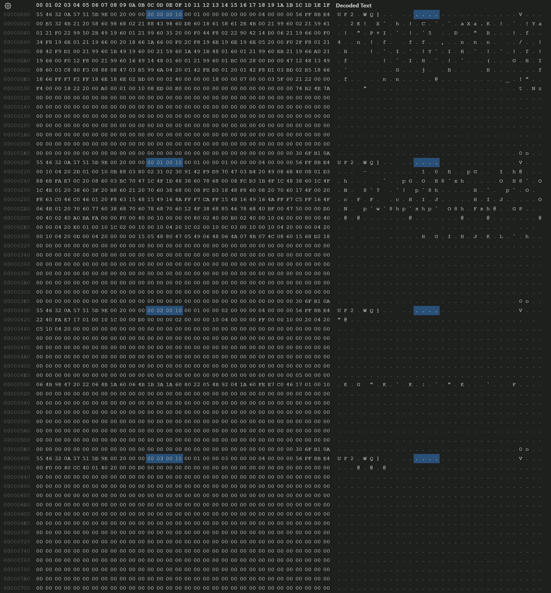
We can also verify the LMA by looking at address field of each block in the uf2 file (highlighted in the following screenshot):
Measure the Output
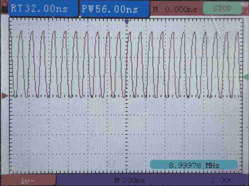
Download the uf2 file. Then, use an oscilloscope to measure the output waveform.
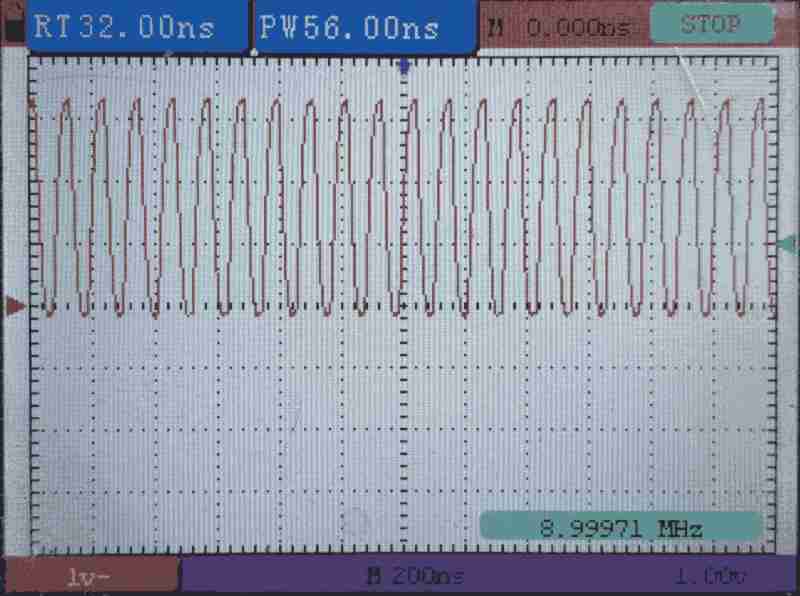
The scope shows a square wave at 9MHz. All green! Our program is running.
Cache Miss in Effect
To verify that a cache miss will stall the process, we adjust the flash read parameter in core 0's program. In a dead loop, we will try to read a number of address from the flash memory space. In case of read hit, we should see the output waveform at the maximum frequency; otherwise, we will see the output frequency lowered.
	ldr	r2, =0x10000000		@ Flash pointer
	ldr	r3, =0x00000004		@ Flash step (must be 4x for word read)
	ldr	r4, =0x100000FF		@ Flash mask

1:	str	r0, [r1, #0]
	ldr	r5, [r2, #0]
	add	r2, r2, r3
	and	r2, r2, r4
	b	1b
We have the following parameters:
r2- Which flash chache strategy to use. 0x10000000 for cacheable and allocatable, 0x13000000 for non-cacheable and non-allocatable (always miss).r3- Step between each flash read.r4- Top of flash read address using mask. Warpback once reached.
All Hit - Fit in cache size
We have the following parameters:
r2- 0x10000000r3- 0x00000004r4- 0x100000FF
which means, we read the following addresses (64 locations):
0x100000000x100000040x100000080x1000000C0x100000100x10000014- ...
0x100000F80x100000FC- Warpback to
0x10000000
We read multiple locations in the flash memory space, and the window is 256 bytes. This is smaller than the XIP cahce size; therefore, all thees locations are cached.
Partial Hit - Frequent cache reload
We have the following parameters:
r2- 0x10000000r3- 0x00000400r4- 0x1000FFFF
which means, we read the following addresses (64 locations):
0x100000000x100004000x100008000x10000C000x100010000x10001400- ...
0x1000F8000x1000FC00- Warpback to
0x10000000
We read multiple locations in the flash memory space, step size is 1 kiB but the window size is 64 kiB. This step size is smaller than the XIP cahce size but the window size is larger than the XIP cache size; therefore, sometimes hit.
All Miss - Step larger than cache size
We have the following parameters:
r2- 0x10000000r3- 0x00004000r4- 0x100FFFFF
which means, we read the following addresses (64 locations):
0x100000000x100040000x100080000x1000C0000x100100000x10014000- ...
0x100F80000x100FC000- Warpback to
0x10000000
We read multiple locations in the flash memory space, step size is 16 kiB. This is larger than the XIP cache size; therefore, all missed.
All Hit - 2 way cached
We have the following parameters:
r2- 0x10000000r3- 0x00080000r4- 0x100FFFFF
which means, we read the following addresses (2 locations):
0x100000000x10080000- Warpback to
0x10000000
Although step is large, but only 2 locations are read. Since the XIP uses 2-way cache, we will not miss.