Switch RP2040 Clock Source in Baremetal: ROSC, XOSC and PLL
Compare the RP2040 clock sources, switch the clock source in bare metal.
Paspberry Pi Pico, RP2040, ARM, Cortex M0+, Assembly, Baremetal, Clock source, Clock tree, ROSC, Ring oscillator, XOSC, crystal oscillator, PLL, Phase locked loop, MCU
--by Captdam @ Mar 8, 2026Index
This article is intended for developers who are familiar with 8-bit MCUs and use Assembly and C language to develop bare metal applications, but new to 32-bit RP2040 and ARM Cortex-M0+.
Since we are creating bare metal applications, we will be directly writing to and reading from the MCU and the external flash device control registers. No library is used.
We will rely on the documents heavily. It includes all information we need about the MCU and the external flash device control registers.
Because of the RP2040 document updates, and for some reason they decided to redirect my links to the old document to the new document, I decided to create a copy of the current version (2025-02-20) on my server. You may obtain this document from the official link here (as 2026-02-10).
The RPI Pico board comes with a flash memory chip to store user program, the W25Q family. Note that the W25Q family has multiple models. They all follow the same SPI communication protocol, but differ in continuation code. The continuation code is a 8-bit code followed by the data address code, used to opt out read command code in subsequent transactions, to reduce data read overhead.
Although the Pico document (copy from offcial link (as 2026-02-10)) says the on-board flash is Winbond W25Q16JV, which uses continuation code 0b1111xxxx, where x stands for do-not-care. I found it different than the continuation code 0b10101010 used in the SDK bootloader. Based on my research, W25Q80EW uses 0bxx01xxxx, matches with the continuation code used in the SDK bootloader. I will use document of this flash for reference in this article.
This article is based on my previous article: RP2040 Baremetal Dual-core Application and Core 1 Launch Protocol, you may want to check it first.
How Fast Is My RP2040 Running
Project file for measuring the CPU clock after power-up can be found here.
As the RP2040 document states, the RP2040 has Dual ARM Cortex-M0+ @ 133MHz, that is, 266 million 32-bit operations in total. Furthermore, You can achieve 200MHz by running at an elevated core supply (DVDD) and setting VREG VSEL to 1.15V, that is, 400 million 32-bit operations in total. This even beats some PCs in the early 2000s.
However, how fast is my RP2040 actually running?
Use SIO to Measure CPU Speed
To find out the answer, we can write a simple assembly program, name the file main.s:
.cpu cortex-m0plus
.thumb
.align 2
.thumb_func
.section .vector
.global vector
vector:
.word 0x20041000
.word reset + 1
.section .text
.global reset
reset:
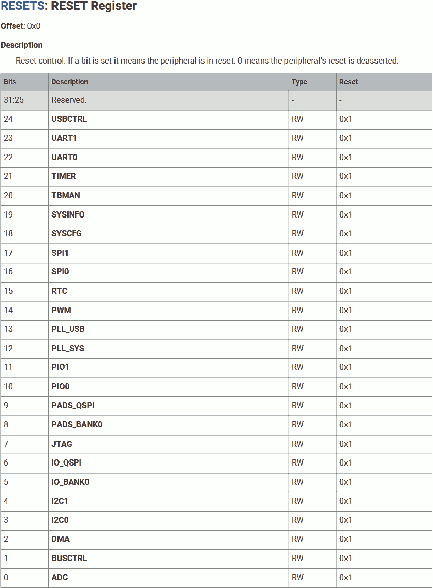
ldr r7, =0x4000f000 @ RESETS_RESET + 0x3000
mov r0, #(1<<5) @ IO_BANK0
str r0, [r7, #0x00]
ldr r7, =0x400140cc @ IO_BANK0_GPIO25_CTRL
mov r0, #5 @ SIO
str r0, [r7, #0x00]
ldr r7, =0xd0000000 @ SIO_GPIO_BASE
ldr r0, =(1<<25) @ GPIO25
str r0, [r7, #0x20] @ SIO_GPIO_BASE_OE
1: str r0, [r7, #0x1C] @ SIO_GPIO_BASE_XOR
b 1b
This program contains a dead loop which XOR the output.
According to the instruction set document:
str r0, [r7, #0x1C]- Writing to the GPIO 25 (SIO) will consume 1 CPU clock cycle.b 1b- Branching with PC modified will consume 2 CPU cycles.
In total, the GPIO 25 flips every 3 CPU cycles, and the wave period will be 6 CPU cycles (3 cycles high, 3 cycles low).
Link for USB Start and Flash Start
To link the program into SRAM and execute the program from SRAM (start after USB downloading), create a linker script sram.ld:
MEMORY {
	SRAM(rwx) : ORIGIN = 0x20000000, LENGTH = 264k
	SRAM_4(rwx) : ORIGIN = 0x20040000, LENGTH = 4k
	SRAM_5(rwx) : ORIGIN = 0x20041000, LENGTH = 4k
	SRAM_0(rwx) : ORIGIN = 0x21000000, LENGTH = 64k
	SRAM_1(rwx) : ORIGIN = 0x21010000, LENGTH = 64k
	SRAM_2(rwx) : ORIGIN = 0x21020000, LENGTH = 64k
	SRAM_3(rwx) : ORIGIN = 0x21030000, LENGTH = 64k
}

ENTRY(reset)

SECTIONS {
	.text : {
		*(reset)
	} > SRAM
}
Only place the reset routine to SRAM. The vector is not required.
The entry point is reset routine.
To link the program into flash and execute the program from flash (start after USB downloading and reloading from flash), allow the program to be preserved after power cycle, create a linker script sram.ld:
MEMORY {
	FLASH(rwx) : ORIGIN = 0x10000000, LENGTH = 2048k
}

SECTIONS {
	.text : {
		*(.boot2)
		*(.vector)
		*(reset)
	} > FLASH
}
Place the 2nd stage bootloader .boot we generated in the previous article at the beginning of flash, as required by the on-chip bootloader. Next, place the vector table vector right after the 2nd stage bootloader, as required by the 2nd stage bootloader. At the end, place the reset routine.
Entry point is not required for flash programming.
Compile
arm-none-eabi-as --warn --fatal-warnings -g main.s -o main.o
arm-none-eabi-objdump --disassembler-options=force-thumb -Dxs main.o > main.list

# SRAM
arm-none-eabi-ld -nostdlib -nostartfiles -T sram.ld main.o -o sram.elf
arm-none-eabi-objdump --disassembler-options=force-thumb -dxs sram.elf > sram.list
pico-elf2uf2 sram.elf sram.uf2

# Flash
arm-none-eabi-ld -nostdlib -nostartfiles -T flash.ld main.o boot2.o -o flash.elf
arm-none-eabi-objdump --disassembler-options=force-thumb -dxs flash.elf > flash.list
pico-elf2uf2 flash.elf flash.uf2
Compile this project. This generates two uf2 files:
sram.uf2- Download and execute from SRAM.flash.uf2- Burn the flash and execute the program from flash, allow the program to be preserved after power cycle.
Measure Frequency
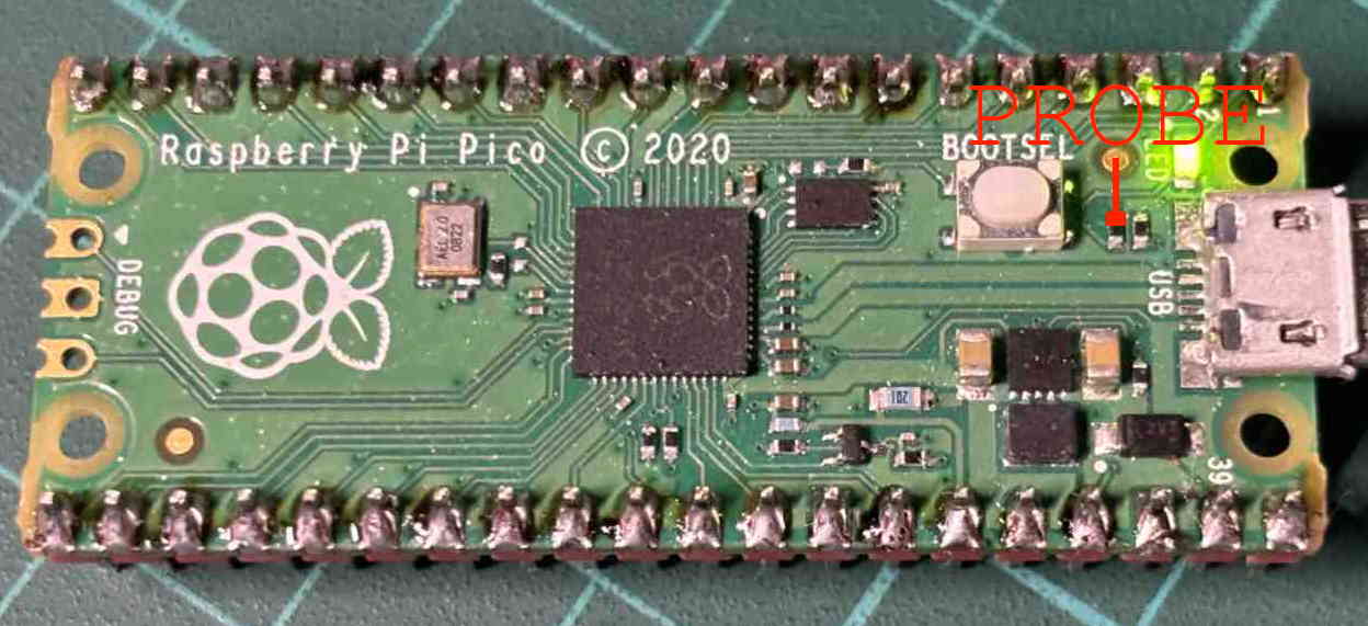
Now, we can use an oscilloscope to measure the output signal. We will measure the signal at this position, at the high end of the LED resistor. See the above figure for the test point.
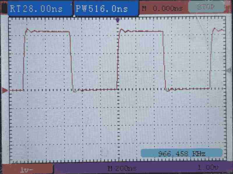
As the scope shows, the signal frequency is around 966kHz. Since the wave period is 6 CPU cycles, the CPU is running at around 5.8MHz.
This is far less than the advertised 133MHz.
Let's try different setting scenarios. We will try:
- Download to SRAM and execute from SRAM.
- Download to flash and execute from flash.
- Download to flash, power cycle, then execute from flash.
| Scenario | Measure Frequency | CPU Speed |
|---|---|---|
| Download to SRAM | 966kHz | 5.8MHz |
| Download to Flash | 966kHz | 5.8MHz |
| Download to Flash then Power Cycle | 966kHz | 5.8MHz |
All scenarios gives 5.8MHz CPU (sys) clock frequency.
Clock Tree
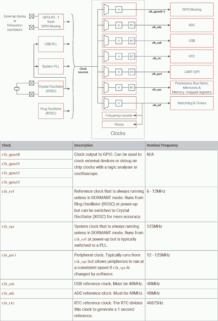
PR2040 provides a set of clock sources. They are shown on the left side of the figure. Note some clock sources are driven by other clock sources.
There are clock generators that select one of the clock sources, then use a divider to decrease the frequency (to save power or to satisfy the consumer’s max frequency). They are shown in the middle of the figure.
The output clock signals are then fed to the consumers, including system (CPU cores), peripherals, clock outputs.
At power-up, reference clock clk_ref is driven from ROSC, and the system clock (CPU) clk_sys is driven from clk_ref (not directly from ROSC).
Clock Options
Some clock outputs can be fed to another clock's input. The detail can be found in the clock generator's control registers. Following is what I had analysis:
CLK_GPIO_0 / CLK_GPIO_1
- CLKSRC_PLL_SYS
- CLKSRC_GPIN0
- CLKSRC_GPIN1
- CLKSRC_PLL_USB
- ROSC_CLKSRC
- XOSC_CLKSRC
- CLK_SYS
- CLK_USB
- CLK_ADC
- CLK_RTC
- CLK_REF
CLKSRC_GPIN0 and CLKSRC_GPIN1 are available for all generators.
CLKSRC_PLL_USB is available for all generators. CLKSRC_PLL_SYS is available for all generators except CLK_REF.
CLK_GPIO_2 / CLK_GPIO_3
- CLKSRC_PLL_SYS
- CLKSRC_GPIN0
- CLKSRC_GPIN1
- CLKSRC_PLL_USB
- ROSC_CLKSRC_PH (phase shift)
- XOSC_CLKSRC
- CLK_SYS
- CLK_USB
- CLK_ADC
- CLK_RTC
- CLK_REF
CLK_GPIO_2 and CLK_GPIO_3 are same as CLK_GPIO_0 and CLK_GPIO_1 except using phase shift of ROSC.
CLK_GPIO_N can use the output of other generators (except CLK_PERI).
CLK_REF
- ROSC_CLKSRC_PH
- CLKSRC_CLK_REF_AUX
- CLKSRC_PLL_USB
- CLKSRC_GPIN0
- CLKSRC_GPIN1
- XOSC_CLKSRC
CLK_SYS
- CLK_REF
- CLKSRC_CLK_SYS_AUX
- CLKSRC_PLL_SYS
- CLKSRC_PLL_USB
- ROSC_CLKSRC
- XOSC_CLKSRC
- CLKSRC_GPIN0
- CLKSRC_GPIN1
CLK_PERI
- CLK_SYS
- CLKSRC_PLL_SYS
- CLKSRC_PLL_USB
- ROSC_CLKSRC_PH
- XOSC_CLKSRC
- CLKSRC_GPIN0
- CLKSRC_GPIN1
CLK_USB / CLK_ADC / CLK_RTC
- CLKSRC_PLL_USB
- CLKSRC_PLL_SYS
- ROSC_CLKSRC_PH
- XOSC_CLKSRC
- CLKSRC_GPIN0
- CLKSRC_GPIN1
Switch Clock Source
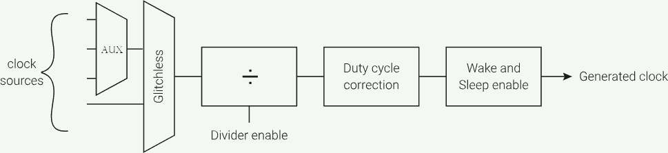
At the input side of the clock generator is a multiplexer that can be used to select the clock source. Most clock generators only have an auxiliary (aux) multiplexer, the reference clock clk_ref and the system clock clk_sys have both aux mux and glitchless mux.
To switch the clock source of an aux mux, its consumer must be stopped due to clock glitch. Furthermore, it requires 2 clock cycles (of the old clock source) to stop and 2 clock cycles (of the new clock source) to restart.
Switching of the glitchless mux can be executed on-the-fly. This allows the CPU to continue running (to perform the switching).
If the glitchless mux is feed from the aux mux and we need to switch the aux mux, we must switch the glitchless mux to another clock source first to avoid signal glitch feed to the glitchless mux (the term "glitchless" only applies to switching). Then, we can perform the switch of aux mux; and next, we can switch the glitchless mux back to the switched aux mux.
Default Clock Source - Ring Oscillator (ROSC)
The ring oscillator is an on-chip clock source that is always available and always used at power-up. This clock source is built inside the RP2040 chip, meaning it does not require any external component nor occupy any pins.
At power-up, this clock source is always selected. This is the safest option. It ensures the system can run when there is no external clock source or when the external source is failed. (On RP2040, it is possible to test a clock while running on anoter clock.)
On a low-cost system, this clock source is favored. It requires no external component; hence, minimize the system cost.
However, this clock is not accurate. Its frequency varies by voltage and temperature.
The frequency can be changed by modifying the related registers.
| Case | RP2040 | AVR (classic) |
|---|---|---|
| Availability | Built-in always available, no external component required | |
| Accuracy | Frequency vary by voltage and temperature | |
| Change frequency | Modify control registers on-the-fly | |
| Default clock source | Default option at power-up | Default option in fuse (non-volatile) |
| Change clock source | Modify clock source register on-the-fly only There is no way to modify on-chip boot ROM. |
Modify the fuse at programming time |
| Chang during run-time | Yes | No, fuse can be changed during programming only Serial or parallel programming only. Does not include bootloader programming or in-system programming. |
| Apply to | CPUs (sys) and peripherals can select different clock source | Whole system, except (Async) Timer / Counter |
More Accurate Clock Source - Crystal Oscillator (XOSC)
Using the crystal oscillator can provide a more accurate and stable clock frequency then ROSC, because the physical characteristics of the crystal can be precisely prepared during manufacturing, and the physical characteristics determine the oscillation frequency. The frequency is nearly independent of voltage and temperature.
It is favored to use the crystal if timing is crucial. For example, using UART.
However, external components (the crystal) are required for this option. This means higher system cost. The Pico board does come with an on-board 12MHz crystal.
Furthermore, the crystal oscillator requires longer start-up time than the ring oscillator. This is not a concern during power-up, it is just a one-time delay at power-up. However, this may be a concern in case of frequent clock start-stop (sleep mode).
Program to Use XOSC
To switch the system clock source to the crystal oscillator, we can reuse the project we used to measure the clock frequency in earlier section of this article, but modify the the file main.s in the following way:
.cpu cortex-m0plus
.thumb
.align 2
.thumb_func

.section .vector
.global vector
vector:
	.word	0x20041000
	.word	reset + 1

.section .text
.global reset
reset:

@ Switch to XOSC
	ldr	r7, =0x40008000
	mov	r0, #((3<<5) | (0<<0))
	str	r0, [r7, #0x3C]
	nop
	nop
	nop
	nop
	mov	r0, #((3<<5) | (1<<0))
	str	r0, [r7, #0x3C]

@ GPIO
	ldr	r7, =0x4000f000		@ RESETS_RESET  + 0x3000
	mov	r0, #(1<<5)		@ IO_BANK0
	str	r0, [r7, #0x00]
	ldr	r7, =0x400140cc		@ IO_BANK0_GPIO25_CTRL
	mov	r0, #5			@ SIO
	str	r0, [r7, #0x00]
	ldr	r7, =0xd0000000		@ SIO_GPIO_BASE
	ldr	r0, =(1<<25)		@ GPIO25
	str	r0, [r7, #0x20]		@ SIO_GPIO_BASE_OE

1:	str	r0, [r7, #0x1C]		@ SIO_GPIO_BASE_XOR
	b	1b
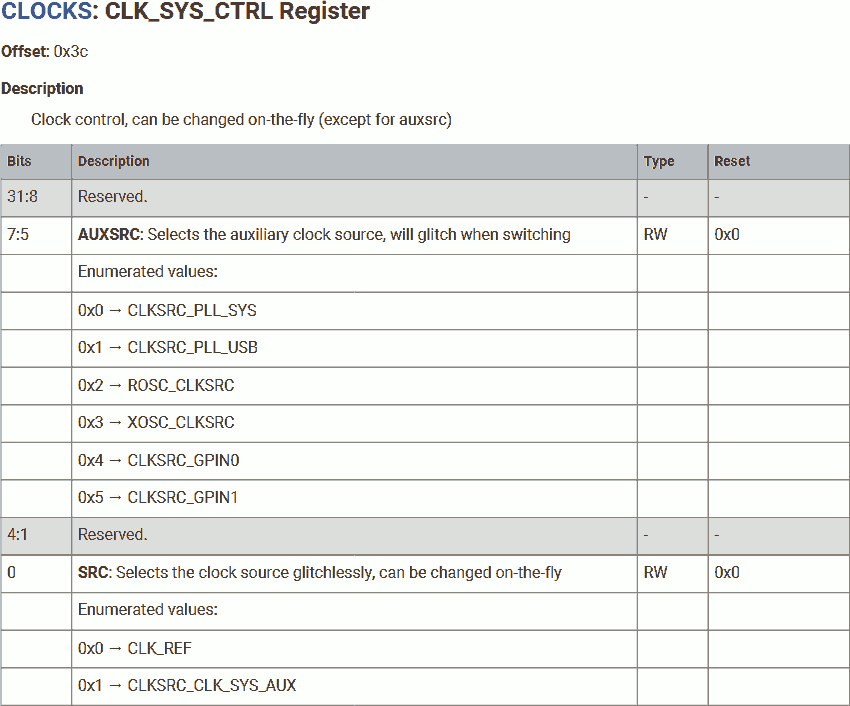
First, change the system clock control register to switch the aux mux and glitchless mux at the same time:
- Change the glitchless mux to use reference clock source. This change can be executed on-the-flay. If the glitchless mux is currently running on the reference clock, this switching has no effect. If the glitchless mux is currently running on the aux mux, this switching gated the will-glitch input.
- Change the aux mux to the desired clock source. In this example, the crystal oscillator.
Wait for 4 cycles (of ROSC). Since ROSC is running at 5.8MHz but the XOSC is running at 12MHz, 4 cycles of ROSC is for sure longer than 2 cycles of ROSC plus 2 cycles of XOSC. Furthermore, loading r0 and writing to the control register also provides extra time.
Now, the aux mux should be stable. We can change the glitchless mux to use the aux mux as its source.
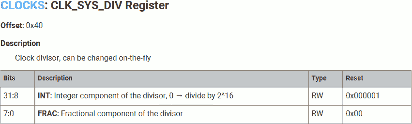
We will use the default clock divider (1).
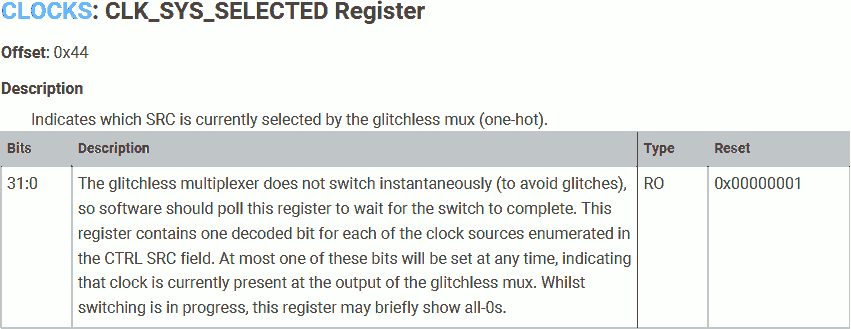
The glitchless multiplexer does not switch instantaneously (to avoid glitches), it takes a few cycles to actually switch the clock source, the CLOCKS_CLK_SYS_SELECTED register can be used to get the current clock to confirm the clock source is switched. We are not concern about this issue in this example.
Measure XOSC Frequency
We can compile this project use the same linker scripts and shell commands. After downloading, measure the output frequency:
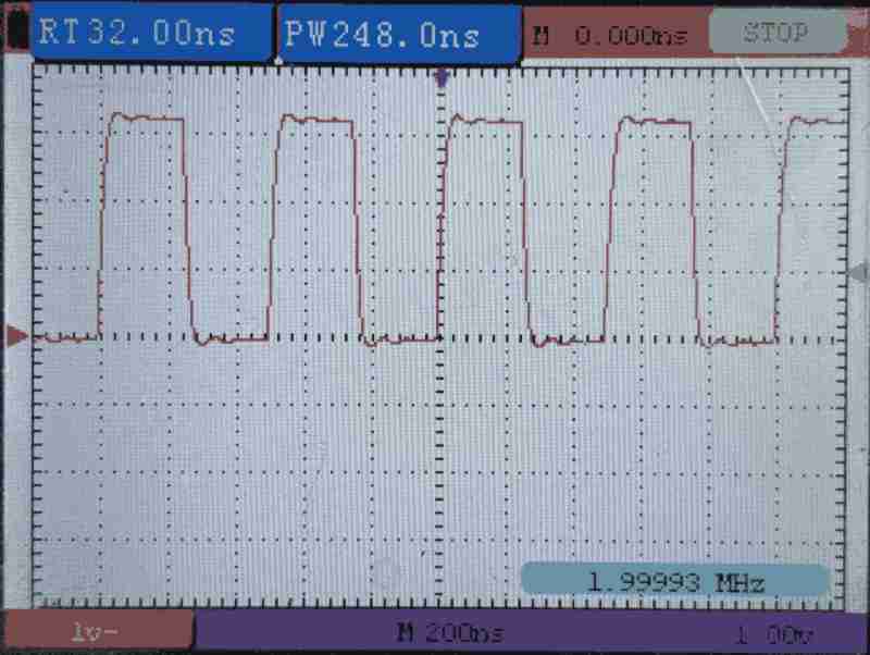
| Scenario | Measure Frequency | CPU Speed |
|---|---|---|
| Download to SRAM | 1.999MHz | 12MHz |
| Download to Flash | 1.999MHz | 12MHz |
| Download to Flash then Power Cycle | 0 | 0 |
Start XOSC
To start the crystal oscillator (XOSC), we will need to modify the the file main.s again in the following way:
.cpu cortex-m0plus
.thumb
.align 2
.thumb_func

.section .vector
.global vector
vector:
	.word	0x20041000
	.word	reset + 1

.section .text
.global reset
reset:

@ Start XOSC
	ldr	r7, =0x40024000
	ldr	r0, =0x00FABAA0
	str	r0, [r7, #0x00]
1:	ldr	r0, [r7, #0x04]
	lsr	r0, #32
	bcc	1b

@ Switch to XOSC
	ldr	r7, =0x40008000
	mov	r0, #((3<<5) | (0<<0))
	str	r0, [r7, #0x3C]
	nop
	nop
	mov	r0, #((3<<5) | (1<<0))
	str	r0, [r7, #0x3C]

@ GPIO
	ldr	r7, =0x4000f000		@ RESETS_RESET  + 0x3000
	mov	r0, #(1<<5)		@ IO_BANK0
	str	r0, [r7, #0x00]
	ldr	r7, =0x400140cc		@ IO_BANK0_GPIO25_CTRL
	mov	r0, #5			@ SIO
	str	r0, [r7, #0x00]
	ldr	r7, =0xd0000000		@ SIO_GPIO_BASE
	ldr	r0, =(1<<25)		@ GPIO25
	str	r0, [r7, #0x20]		@ SIO_GPIO_BASE_OE

1:	str	r0, [r7, #0x1C]		@ SIO_GPIO_BASE_XOR
	b	1b
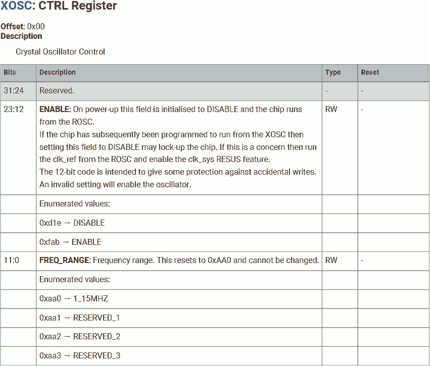
To start XOSC, set the XOSC_CTRL register with ENABLE password and FREQ_RANGE, where the ENABLE must be 0xFAB and FREQ_RANGE must be 0xAA0.
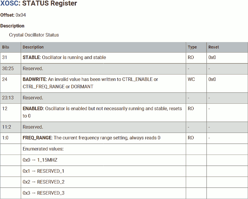
Then, poll the STABLE bit in XOSC_STATUS until the XOSC clock is stable.
Now, XOSC can be used.
Once linked and compiled, the XOSC works even after power cycle.
Project file for starting and switching to XOSC can be found here.
Run Faster - Phase Locked Loop (PLL)
For even higher frequency, we will need to use PLL.
There are two PLLs in RP2040, system PLL and USB PLL. As the name suggests, the system PLL is intended for the system use (CPU, SRAM, IO, peripherals), and the USB PLL is for USB. This allows the system and USB to be running at two different frequencies. FOr example, the system is running at up to 133MHz while the USB is running at 48MHz.
If both the system and the USB are running at the same frequency, both can use the same PLL to save power.
To use the PLL:
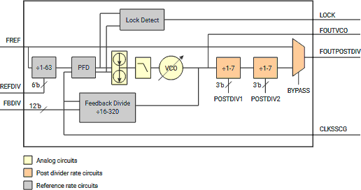
- The PLL is hard wired to XOSC, the XOSC is usde as the reference clock. Therefore, XOSC must be enabled. ROSC cannot be used because ROSC is not stable; hence, cannot be "locked".
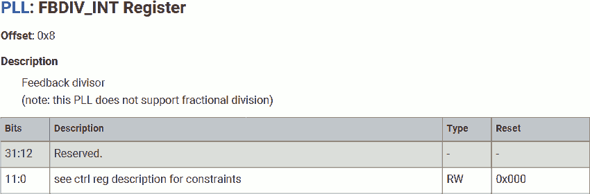
- Set the feedback divider. The VCO stage must be in the range of 750MHz to 1.6GHz. Higher VCO frequency means lower jitter, while lower VCO frequency means lower power consumption.
- Set the 2-stage post divider to generate the desired system / USB frequency. The maximum system frequency is 133MHz and the maximum USB frequency is 48MHz.
Following shows some PLL settings:
| Target frequency | Feedback divider | VCO Frequency | Post divider 1 | Post divider 2 | Actual frequency | Comments |
|---|---|---|---|---|---|---|
| 133MHz | 133 | 1596MHz | 6 | 2 | 133MHz | Perfect! |
| 133MHz | 133 | 1596MHz | 2 | 6 | 133MHz | Swap the two post dividers to reduce the frequency between them to save power. |
| 133MHz | 66 | 792MHz | 6 | 1 | 132MHz | Slightly off, but save a great deal of power at VCO. |
Program to Use System PLL
To switch the system clock source to the system PLL, we can reuse the project we used to use XOSC in earlier section of this article, but modify the the file main.s in the following way:
Enable XOSC
.cpu cortex-m0plus
.thumb
.align 2
.thumb_func

.section .vector
.global vector
vector:
	.word	0x20041000
	.word	reset + 1

.section .text
.global reset
reset:

@ Start XOSC
	ldr	r7, =0x40024000
	ldr	r0, =0x00FABAA0
	str	r0, [r7, #0x00]
1:	ldr	r0, [r7, #0x04]
	lsr	r0, #32
	bcc	1b
The system PLL and the USB PLL need to use the XOSC as their reference clock. Thereore, we will need to enable XOSC first. Detail of this code can be found in the previous example.
Allow PLL
@ Start PLL
	ldr	r7, =0x4000f000
	ldr	r0, =(1<<12)
	str	r0, [r7, #0x00]
After power-up, the system PLL is in reset. We will need to write 1 to bring the system PLL out of reset. To preserve the reset status of other components, add 0x3000 to the address for atomically write to clear.
Configurate VCO
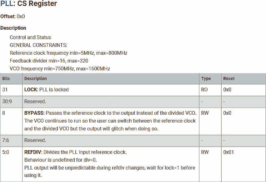
	ldr	r7, =0x40028000
	ldr	r6, =0x40028000 + 0x3000
	mov	r0, #(1<<0)
	str	r0, [r7, #0x00]
	mov	r0, #66
	str	r0, [r7, #0x08]
RP2040 comes with two of PLLs, one for system that runs up to 133MHz; another one for USB that runs up to 48MHz. The base address is 0x40028000 for system PLL control registers; and 0x4002C000 for USB PLL control registers.
We will use r7 for base address of the system PLL control registers, use r6 for atomically write to clear system PLL control registers.
First, set the reference clock divider to 1. Since the on-board crystal is 12MHz, this will bring 12MHz / 1 = 12MHz reference signal into the PLL. This setting is helpful if the chip is driven by high frequency clock.
Then, set the feedback divider to 66. This will bring the frequency at VCO to 12MHz * 66 = 792MHz.
Start PLL
	mov	r0, #((1<<5) | (1<<0))
	str	r0, [r6, #0x04]
1:	ldr	r0, [r7, #0x00]
	lsr	r0, r0, #32
	bcc	1b
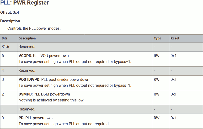
By default, all components in the PLL is powered down. Power-up the VCO and the the PLL to start the PLL, but keep the post divider down.
It takes a while for the frequency to stable and the phase to locked. We can poll the LOCK bit in the PLL_SYS_CS register to confirm when the PLL is ready.
Configurate post divider
	ldr	r0, =((6<<16) | (1<<12))
	str	r0, [r7, #0x0C]
	mov	r0, #(1<<3)
	str	r0, [r6, #0x04]
Set the 2-stage post divider. We use 6 for the first stage and 1 for the second stage, this brings the frequency down to 792MHz / 6 / 1 = 132MHz.
Power up the post divider.
Switch to PLL
@ Switch to PLL
	ldr	r7, =0x40008000
	mov	r0, #((0<<5) | (0<<0))
	str	r0, [r7, #0x3C]
	nop
	nop
	mov	r0, #((0<<5) | (1<<0))
	str	r0, [r7, #0x3C]
Switch the aux and glitchless mux to use the system PLL. Detail of this code can be found in the previous example.
GPIO
@ GPIO
	ldr	r7, =0x4000f000		@ RESETS_RESET  + 0x3000
	mov	r0, #(1<<5)		@ IO_BANK0
	str	r0, [r7, #0x00]
	ldr	r7, =0x400140cc		@ IO_BANK0_GPIO25_CTRL
	mov	r0, #5			@ SIO
	str	r0, [r7, #0x00]
	ldr	r7, =0xd0000000		@ SIO_GPIO_BASE
	ldr	r0, =(1<<25)		@ GPIO25
	str	r0, [r7, #0x20]		@ SIO_GPIO_BASE_OE

1:	str	r0, [r7, #0x1C]		@ SIO_GPIO_BASE_XOR
	b	1b
Configurate the GPIO and flip the output.
Measure System PLL Frequency
We can compile this project use the same linker scripts and shell commands. After downloading, measure the output frequency:
| Scenario | Measure Frequency | CPU Speed |
|---|---|---|
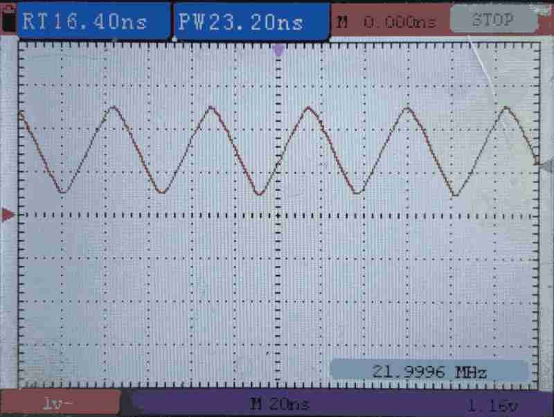
| Download to SRAM | 22MHz | 132MHz |
| Download to Flash | 22MHz | 132MHz |
| Download to Flash then Power Cycle | 22MHz | 132MHz |
Project file for starting and switching to PLL can be found here.
How Fast Can W25Q Flash Running
Now, we successfully clock the RP2040 to 133MHz. Before we end this article, we would like to ensure the external devices (most importantly, the on-board W25Q flash) is fast enough.
The W25Q flash supports both "standard" read and "fast" read, where:
The max SPI frequency allowed in "standard" read is 50MHz and in "fast" read is 133MHz (3.0V) or 104MHz (2.7V).
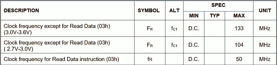
Recall, in the SDK 2nd-stage, the SSI BAUD is set to 2. This means, the SSI perform a write or sample at 133MHz / 2 = 67.5MHz. Furthermore, write and read are perform on the opposite edge of the SPI clock, which means the SPI clock frequency is half of 67.5MHz, that is 33.25MHz. This is lower than the max frequency of W25Q. We are safe!
In my next article, we will Compare RP2040 Executable Memory Regions and Load Program From Flash into SRAM.