RP2040 Baremetal Dual-core Application and Core 1 Launch Protocol
Analysis the RP2040 Core 1 launch protocol. Launch core 1 in bare metal multi-processor application with minimum code.
Paspberry Pi Pico, RP2040, ARM, Cortex M0+, Assembly, Baremetal, Bootloader, MCU, Dualcore, Multi-processor
--by Captdam @ Mar 7, 2026Index
This article is intended for developers who are familiar with 8-bit MCUs and use Assembly and C language to develop bare metal applications, but new to 32-bit RP2040 and ARM Cortex-M0+.
Since we are creating bare metal applications, we will be directly writing to and reading from the MCU control registers. No library is used.
We will rely on the documents heavily. It includes all information we need about the MCU control registers.
Because of the RP2040 document updates, and for some reason they decided to redirect my links to the old document to the new document, I decided to create a copy of the current version (2025-02-20) on my server. You may obtain this document from the official link here (as 2026-02-10).
This article is based on my previous article: W25Q Flash and RP2040 SDK Bootloader in Baremetal, you may want to check it first.
On-chip Boot ROM
The RP2040 is a dual-core MCU. After the on-chip bootloader exits, CPU 0 starts to execute the user program saved in flash or loaded from USB, CPU 1 sleeps.
For maximum performance, we would like to use both CPUs. To do so, we need to wake-up the second CPU first.
First, let's take a look at how the second CPU (Core 1) is put into sleep during the on-chip bootloader stage.
You can find the code related to core 1 sleep and wake-up protocol here.
Enter Sleep Mode
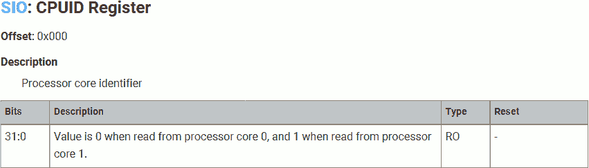
CPU ID
.global _start
.type _start,%function
.thumb_func
_start:

check_core:
	ldr r0, =SIO_BASE
	ldr r1, [r0, #SIO_CPUID_OFFSET]
	cmp r1, #0
	bne wait_for_vector
	bl _nmi
On power up, both cores start the same on-chop bootloader. It relies on the CPU ID to determine which core the program is running on. If the CPU ID is 0 (Core 0), continue the on-chip bootloader; if 1 (Core 1), go to the core 1 wait (sleep) routine.
This is similar to the pid_t pid = fork() system call on Linux, where we use pid to determine whether we are in the parent process or child process.
Note that each core has its own private CPU control registers. Core 0 can access core 0’s CPU control registers only; core 1 can access core 1’s CPU control registers only. That means, both cores read the same address 0xD0000000 for CPU ID, but the value returned is from the core’s local registers, and the value is different.
If the returned value (CPU ID) is zero, that means we are running on Core 0. We will continue to routine _nmi. This program is out of this article’s scope.
If the returned value is non-zero, that means we are running on Core 1. We will continue to wait_for_vector.
Sleep Mode
wait_for_vector:
ldr r4, =SIO_BASE
ldr r7, =M0_BASE
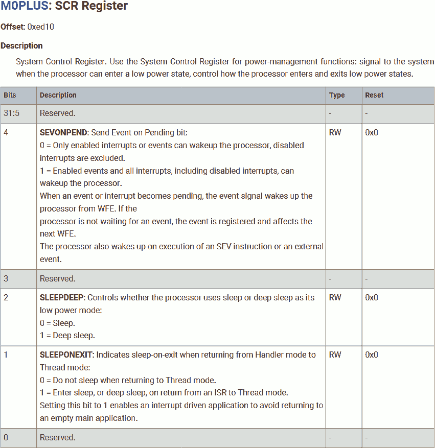
mov r1, #M0PLUS_SCR_SLEEPDEEP_BITS
str r1, [r7, #(M0PLUS_SCR_OFFSET - M0PLUS_CPUID_OFFSET)]
Set the deep sleep bit in the system control register to allow core 1 entering deep sleep mode when waiting for events.
r4 is used as SIO control register base address and r7 is used as CPU control register base address in subsequent operations.
Your device might include a Wakeup Interrupt Controller (WIC), an optional peripheral that can detect an interrupt and wake the processor from deep sleep mode. The WIC is enabled only when the DEEPSLEEP bit in the SCR is set to 1. The WIC is not programmable, and does not have any registers or user interface. It operates entirely from hardware signals. -- Cortex-M0+ Devices Generic User Guide: 2.5.3 The optional Wakeup Interrupt Controller
The Wakeup Interrupt Controller (WIC) is used to wake the processor from a DEEPSLEEP state as controlled by the SCR register. The WIC takes inputs from the receive event signal (from the other processor), 32 interrupts lines, and NMI. -- RP2040 Datasheet: 2.4.2.8.4. Wakeup Interrupt Controller
That means: Writing to mailbox from core 0 to core 1 while core 1 is in deep sleep mode will send a event to core 1.
Clear the Inter-processor Mailbox FIFO
1:
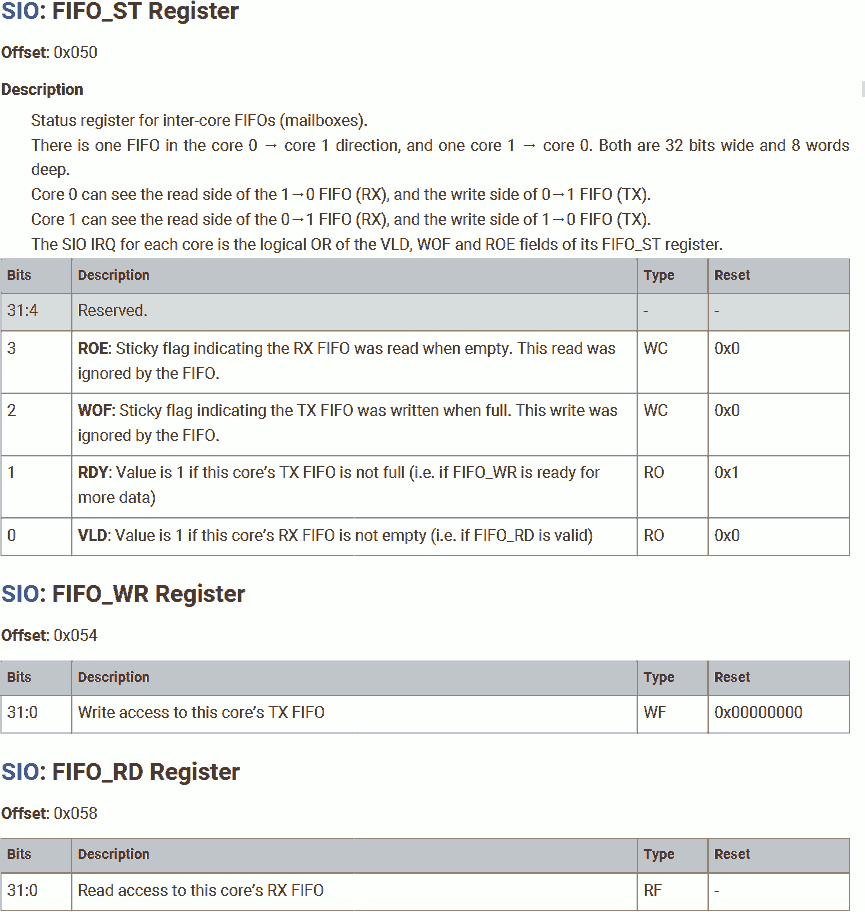
ldr r1, [r4, #SIO_FIFO_RD_OFFSET]
core_0_handshake_loop:
ldr r1, [r4, #SIO_FIFO_ST_OFFSET]
lsr r1, #SIO_FIFO_ST_VLD_LSB + 1
bcs 1b
Use the mailbox (FIFO) to send messages from one core to another. There are two one-way mailboxes, data written to the mailbox by one core can only be read from the mailbox by another core, and vice versa.
In most cases, the mailbox should be empty after a fresh start (power-up reset). But in some rare cases, there may be unread messages in the mailbox. To be safe, we will clear the mailbox by reading out all unread messages. This procedure can be described by:
- Check the
VLDbit in the mailbox status register. The valid bit is set when there are 1 or more messages waiting for reading in the mailbox (from core 0 to core 1). - If valid, read a message from the mailbox.
- Repeat the above steps. Until the mailbox is drained.
The on-chip boot ROM did some microoptimization. It reads a message from the mailbox regardless of the mailbox validation, to save some ROM space. This is harmless. Reading an empty mailbox FIFO won't affect the FIFO content, but set the ROE flag. As long as we don't enable ROE interrupt, this won't cause any issue.
Handshake Protocol
Send 0, Expect 1
	adr r5, receive_and_check_zero
	mov r0, #0
	bl send_and_then
	cmp r0, #1
	bne core_0_handshake_loop
Use r5 as a function pointer, load it with the subroutine receive_and_check_zero. Thie subroutine is used to read a message from the Inter-processor mailbox FIFO, including protocol header "1", vector table address, initial stack pointer value and entry point.
None of the message should be "0". If the message received from core 0 is "0", restart the protocol by jumping back to core_0_handshake_loop mentioned earlier in Clear the Inter-processor Mailbox FIFO.
This function pointer is used in subsequent operations.
Load message "0" into r0. Then, use r0 as argument register, call send_and_then to send this message to core 0, discussed later here. Next, send_and_then branches to the subroutine saved in function pointer r5, that is, receive_and_check_zero to receive a message, discussed later here. At the end, it returns the received message from core 0 in r0.
The returned message must be "1". Otherwise, redo the above tasks by jumping back to core_0_handshake_loop mentioned earlier in Clear the Inter-processor Mailbox FIFO.
Echo 1, Receive Vector Table Address
	bl send_and_then
	str r0, [r7, #(M0PLUS_VTOR_OFFSET - M0PLUS_CPUID_OFFSET)]
Keep the message from core 0, which is "1". Call send_and_then to send back this message to core 0, which then branches to receive_and_check_zero to receive a message from core 0.
The returned message will be used as the vector table address for core 1.
Echo Vector Table Address, Receive Initial Stack Pointer Value
	bl send_and_then
	msr msp, r0
Keep the message from core 0, which is the vector table address. Call send_and_then to send back this message to core 0, which then branches to receive_and_check_zero to receive a message from core 0.
The returned message will be used as the initial stack pointer value for core 1.
Echo Initial Stack Pointer Value, Receive Entry Point
	bl send_and_then
	; Keep r0
Keep the message from core 0, which is the initial stack pointer value for core 1. Call send_and_then to send back this message to core 0, which then branches to receive_and_check_zero to receive a message from core 0.
The returned message will be used as the entry point for core 1.
Echo Entry Point, Start Main Program for Core 1
	adr r5, core1_launch
	bl send_and_then
Reload function pointer r5 with the subroutine core1_launch. Thie subroutine is start the program for core 1 (core 1 branch to given entry point).
Keep the message from core 0, which is the entry point for core 1. Call send_and_then to send back this message to core 0, which then branches to core1_launch to start the program for core 1, discussed later here.
Handshake Protocol Subroutine
Following are the subroutine used in the handshake protocol:
Send - send_and_then
send_and_then_again:
	wfe
send_and_then:
	ldr r1, [r4, #SIO_FIFO_ST_OFFSET]
	lsr r1, #SIO_FIFO_ST_RDY_LSB + 1
	bcc send_and_then_again
	str r0, [r4, #SIO_FIFO_WR_OFFSET]
	sev
	add r6, r5, #1
	bx  r6
The entry point for this subroutine is send_and_then!
Check the RDY bit in the mailbox status register. The ready bit is set when there is 1 or more space in the mailbox for new messages (from core 1 to core 0).
When logically shifting right, the carry bit is placed on the right side of the 0-th bit of the register.
Shifting the register N + 1 times right will put the N-th bit of that register into the carry bit.
If not ready, which means the mailbox is full. Jump to send_and_then_again. Then, issue a wfe instruction. This stalls core 1, putting core 1 into sleep mode to save power. Once core 0 reads the mailbox, core 1 resumes, and rechecks the RDY bit.
If ready, write the message (in r0) into the mailbox. Then, issue a sev instruction to send an event to core 0 to notify core 0 a new message is available.
Core 1 is in deep sleep mode, the WIC is enabled. A new message will wake core 1 up.
Core 0 may or may not be in deep sleep mode, the WIC may or may not be enabled. Core 1 needs to send an event to wake core 0 up if core 0 is in non-deep sleep mode.
Branch and exchange to the address in function pointer r5 + 1. Thumb instruction requires the LSB of instruction address to be set; so, we add 1 to it.
Receive - receive_and_check_zero
receive_and_check_zero:
	wfe
	ldr r0, [r4, #SIO_FIFO_ST_OFFSET]
	lsr r0, #SIO_FIFO_ST_VLD_LSB + 1
	bcc receive_and_check_zero
	ldr r0, [r4, #SIO_FIFO_RD_OFFSET]
	cmp r0, #0
	beq core_0_handshake_loop
	bx  lr
Wait for an event. This puts core 1 into sleep to save power. When message available, the WIC wakes up core 1.
Check the VLD bit in the mailbox status register. If not set, it means no message from core 0, wait for the event again. (Core 1 may be wake up by other events)
If the received message is "0", redo the above tasks by jumping back to core_0_handshake_loop mentioned earlier in Clear the Inter-processor Mailbox FIFO.
Message from core 0 including protocol header "1", vector table address, initial stack pointer value and entry point. None of the message should be "0":
- Protocol header must be "1".
- Address 0x00000000 - 0x0FFFFFFF is for BOOT ROM, user program should not be in this region; hence the user program vector table address and entry point.
- Initial stack pointer value should be the top of a readable-writable general-purpose memory region. 0 is the top of memory region 0xFFFFFFFF-, which is not sutiable.
If non-zero, return from this subroutine, continue to the next step. Note the received message is saved in r0.
Entry point - core1_launch
core1_launch:
	mov r1, #0
	str r1, [r7, #(M0PLUS_SCR_OFFSET - M0PLUS_CPUID_OFFSET)]
	blx r0
Disable deep sleep mode.
Jump to the entry point saved in r0.
Start Core 1 From Core 0
To start core 1, we need to send the start command to core 1 from core 0 following the protocol discussed above.
The Protocol
| Sequence | We expect (message from core 1 to core 0) | then: We send (message from core 0 to core 1) |
|---|---|---|
| 0 | "0" | "1" |
| 1 | (echo) "1" | Vector table address |
| 2 | (echo) Vector table address | Initial stack pointer value |
| 3 | (echo) Initial stack pointer value | Entry point |
| 4 | (echo) Entry point |
If we send "0" at any time, the protocol restarts.
The SDK Process
According to the manual, the SDK will do the following to start core 1:
const uint32_t cmd_sequence[] = {0, 0, 1, (uintptr_t) vector_table, (uintptr_t) sp, (uintptr_t) entry};

uint seq = 0;
do {
	uint cmd = cmd_sequence[seq];
	if (!cmd) {
		multicore_fifo_drain();
		__sev();
	}
	multicore_fifo_push_blocking(cmd);
	uint32_t response = multicore_fifo_pop_blocking();
	seq = cmd == response ? seq + 1 : 0;
} while (seq < count_of(cmd_sequence));
The SDK:
- Drain the mailbox FIFO and send "0" twice. This effectively resets the mailbox and the protocol to the initial state.
- Send "1".
- Send the vector table address.
- Send the initial stack pointer value.
- Send the entry point.
If the echo from core 1 is different than the message sent, restart the protocol. This is helpful if the core 1 is not in sync with core 0.
Minimum Process
After a fresh power-up reset, we are sure that the core 1 is waiting for the start protocol, the mailbox FIFO is empty (except a "0" message in the mailbox from 1 to core 0), and it is waiting for the first message, protocol header "1". Therefore, we can start core 1 in a quick and dirty way.
Let's use an example to illustrate this process:
Project file for this article can be found here.
Program Code
In a C language file main.c, we will have:
#include <stdint.h>

void c0_reset();
void c1_reset();

uint32_t c0_vector[48] __attribute__ ((section (".c0_vector"))) = {
	0x20041000,
	(uint32_t)c0_reset
};

uint32_t c1_vector[48] __attribute__ ((section (".c1_vector"))) = {
	0x20042000,
	(uint32_t)c1_reset
};

void c0_reset() {
	*(uint32_t volatile * const)(0x4000f000) = (1<<5);
	*(uint32_t volatile * const)(0x400140cc) = 5;
	*(uint32_t volatile * const)(0xd0000020) = (1<<25);

	*(uint32_t volatile * const)(0xd0000054) = 1;
	*(uint32_t volatile * const)(0xd0000054) = (uint32_t)c1_vector;
	*(uint32_t volatile * const)(0xd0000054) = c1_vector[0];
	*(uint32_t volatile * const)(0xd0000054) = c1_vector[1];
	asm("sev\n\t");

	for(;;);
}

void c1_reset() {
	for (;;) {
		*(uint32_t volatile * const)(0xd000001c) = (1<<25); // XOR
		volatile uint32_t dummy;
		for (uint32_t i = 100000; i; i--) {
			dummy++;
		}
	}
}
First, we will define two arrays as the vector table for each core. As we discussed in previous articles, the vector table for RP2040 contains 48 32-bit vectors; therefore, we will use uint32_t[48]:
- The first vector is the initial stack pointer for each processor. We will use SRAM back 4 (address 0x20040000 - 0x20040FFF, 4k size) for core 0 and SRAM bank 5 (address 0x20041000 - 0x20041FFF 4k size) for core 1.
- The second vector is the entry point for that core, or in other words, the address of the main program. The program running on core 0 is
c0_rest, and the program running on core 1 isc1_reset.
Name the vector table section c0_vector and c1_vector for core 0 and core 1, respectively. This is important because the address of the vector table is crucial.
For thumb instruction, the LSB of the instruction address must be set. The compiler did this for us automatically. We can verify this by look into the disassembled code:
10000100 1<c0_vector1>:
10000100:	1000 2004
10000104:	02c1 1000
	...

100002c0 1<c0_reset1>:
100002c0:	2220      	movs	r2, #32
	...
where c0_vector1[1] is 0x100002c1 (LSB is 1), and address of c0_reset1 is 100002c0 (LSB is 0).
Next, define the programs running on both cores:
- The program running on core 0 is
c0_reset1. In this program, we will configure the GPIO mode to allow output as SIO, but will not perform any actual output. This program also launches core 1. - The program running on core 1 is
c1_reset1. In this program, we will blink the LED output on GPIO 25, without configuring it.
To generate some delay, we will increment a dummy variable 100000 times between XOR the output signal. We must declear this dummy variable volatile to disable optimization; otherwise, the complier will increment this dummy variable by 100000 in a single shot.
Both programs must be executed to be able to have visible effect.
We do not need to provide section names for the program. They will be placed in the text section by default.
Linker Script
In a linker script file flash.ld, we will have:
MEMORY {
	FLASH(rx)  : ORIGIN = 0x10000000, LENGTH = 2048k
}

SECTIONS {
	.text : {
		*(.boot2)
		. = ALIGN (256);
		KEEP(*(.c0_vector))
		. = ALIGN (256);
		KEEP(*(.c1_vector))
		KEEP(*(.text))
	} >FLASH
}
Burn the program into flash (address starting from 0x10000000, size 2M).
As required by the on-chip bootloader, the first 256 bytes in the flash (address 0x10000000 - 0x100000FF) must be the 2nd stage bootloader with checksum. In this example, we will use the SDK 2nd stage bootloader. We can reuse the object file boot2.o we generated in the previous article.
As required by the SDK 2nd stage bootloader, immediately after the 2nd stage bootloader is the vector table for core 0. That is, c0_vector. The SDK 2nd stage bootloader will set core 0's stack pointer and launch core 0's main program using content in this vector table.
As required by ARM Cortex M0+ specification, the vector table must be 256-byte aligned. We will place the vector table for core 1 c1_vector in the next 256-byte aligned address. Our program running on core 0 will send data in this vector table via inter-processor mailbox to core 1 to launch core 1.
Because the entire flash region is executable, the instruction text can be placed anywhere as long as it fits into the 2M flash memory and 2-byte aligend. We will place all unallocated text (program instructions) right after c1_vector.
Compile
Compile this project:
arm-none-eabi-gcc -mcpu=cortex-m0plus -c -O3 main.c -o main.o
arm-none-eabi-objdump --disassembler-options=force-thumb -Dxs main.o > main.list

arm-none-eabi-ld -nostdlib -nostartfiles -T flash.ld boot2.o main.o -o flash.elf
arm-none-eabi-objdump --disassembler-options=force-thumb -Dxs flash.elf > flash.list

pico-elf2uf2 flash.elf flash.uf2
Download the uf2 file to Pico.
Burn the program into flash (address starting from 0x10000000, size 2M).
After power-up, the on-chip bootloader will load the 2nd stage bootloader into flash memory space address 0x10000000 - 0x100000FF, and execute from there.
The 2nd stage bootloader configures the SSI to allow execution in place (XIP) from external flash devices, and map the flash device to the 2MiB flash memory space starting from 0x10000000, and launch core 0’s main program from here.
Core 0’s main program will launch core 1. Now, both cores are running on their respective main program.
Note, both cores executed in the XIP memory space, core 0 uses SRAM bank 4 for stack; core 1 uses SRAM bank 5 for stack.
In my next article, we will discuss how to start and switch to RP2040 core clocks, including the ROSC, XOSC and PLL.