W25Q Flash and RP2040 SDK Bootloader in Baremetal
Analysis the W25Q flash memory communication and the RP2040 SDK 2nd stage bootloader in disassembled code from the perspective of an 8-bit MCU developer's view.
Paspberry Pi Pico, RP2040, Flash, W25Q, ARM, Cortex M0+, Assembly, Baremetal, Bootloader, MCU, XIP, SSI, SDK
--by Captdam @ Mar 7, 2026Index
This article is intended for developers who are familiar with 8-bit MCUs and use Assembly and C language to develop bare metal applications, but new to 32-bit RP2040 and ARM Cortex-M0+.
Since we are creating bare metal applications, we will be directly writing to and reading from the MCU and the external flash device control registers. No library is used.
We will rely on the documents heavily. It includes all information we need about the MCU and the external flash device control registers.
Because of the RP2040 document updates, and for some reason they decided to redirect my links to the old document to the new document, I decided to create a copy of the current version (2025-02-20) on my server. You may obtain this document from the official link here (as 2026-02-10).
The RPI Pico board comes with a flash memory chip to store user program, the W25Q family. Note that the W25Q family has multiple models. They all follow the same SPI communication protocol, but differ in continuation code. The continuation code is a 8-bit code followed by the data address code, used to opt out read command code in subsequent transactions, to reduce data read overhead.
Although the Pico document (copy from offcial link (as 2026-02-10)) says the on-board flash is Winbond W25Q16JV, which uses continuation code 0b1111xxxx, where x stands for do-not-care. I found it different than the continuation code 0b10101010 used in the SDK bootloader. Based on my research, W25Q80EW uses 0bxx01xxxx, matches with the continuation code used in the SDK bootloader. I will use document of this flash for reference in this article.

Project file for this article can be found here.
This article is based on my previous article: Raspberry Pi Pico (RP2040) SRAM and Flash Programming, you may want to check it first.
Bootloader
What is a bootloader?
Bootloader is a small program that is used to load the main program to allow the main program to be executed.
As we discussed in my previous article, the on-chip bootloader will only load 256 bytes of data from flash (including 4 bytes of checksum), that is, only 126 Thumb instructions (2 bytes each). This is far less than the space to store a reasonable program.
Therefore, we have to introduce the second stage bootloader (boot2) that fits into the 256-byte space, saved in flash. Its only purpose is to prepare the main program execution.
In conclusion, the on-chip bootloader (manufacturer supplied, saved in on-chip ROM) will load the second stage bootloader (provided by us, saved in flash), which then loads the main program (provided by us, saved in flash).
RP2040 Peripherals
I think it is worth to mention the peripherals used in the bootloader. They are very different than the peripherals we have on 8-bit MCUs.
SSI (Synchronous Serial Interface)
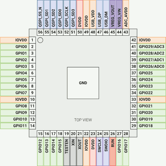
RP2040 pin 56 - 51 supports QSPI and is used as SSI port. It is connected to the on-board flash.
From a 8-bit MCU developer's perspective, the SSI is an advanced SPI. Most importantly:
- It supports not only standard SPI (one input, one output), but also DSPI and QSPI (2 or 4 bidirectional data wire). Since QSPI uses 4 bidirectional data wire, it provides faster transmission speed than standard SPI which has only 1 data wire for one direction.
- It automatically pulls down / up the slave select signal. Unlike the 8-bit MCUs, we have to manually do so.
- It has a deeper buffer. We can send multiple words, then read multiple words. Unlike the 8-bit MCUs with no buffer or 1-word buffer, we have to read one word before sending the next word, or risking the received word being overwritten.
- Write and read are 32-bit wide. Therefore, to send 32-bit data, we only write once. Unlike the 8-bit MCUs, we have to write 4 times.
- We can set frame size. If the frame size is less than 32-bit, the higher bits will be discarded.
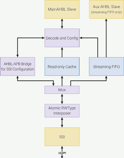
- It has built-in control logic designed for EEPROM. Once configured as XIP, it automatically sends EEPROM instruction and address, and receive EEPROM data.
XIP (Execute in Place)
RP2040 provides a special peripheral called XIP.
In general, the program must be placed in a memory that is accessible for the CPU execution unit.
- For 8-bit MCUs like AVR and 8051, the CPU execution unit is directly connected to the program ROM.
- For PCs, the program is saved on disk. When we execute a program, the operating system will load the program from the disk to the main memory. Then, the CPU can execute the program. Although logically we can
mmap()a file on disk into the memory, the data must be physically copied into main memory from disk. - For Pico with RP2040 MCU, the program is stored in the on-board flash memory connected to the SSI port. To execute the program, it must be copied from the flash into the memory through SSI.
We will need to create a bootloader to copy the program from external flash to the memory through the SSI port. We can manually copy the program from the flash into the memory. Or, we can map the flash into the RP2040 memory space.
RP2040 provides a special peripheral called XIP. It maps the external flash into a memory region, the XIP cache (address 0x10000000 to 0x1FFFFFFF), allowing the CPU to directly execute the program in it.
XIP makes the flash logically a part of the memory. So, the CPU can execute the program in that XIP cache just like it execute from real internal SRAM. The underlying XIP headwear will silently copy the program from the external flash into the XIP cache.
SDK Bootloader
To learn the second stage bootloader, let's check the content of the official SDK's 2nd stage bootloader, source code can be found here. However, this source code is not really easy to read. It includes tons of other files; personally, I don't like it. It is a dependency hell.
Rather, I will disassemble an executable. (If you worked with 8-bit MCUs a lot, you probably perfer to disassemble the binary rather than dig the source code.) The one I choose is the blink program in pico-example/blink. Use arm-none-eabi-objdump --disassembler-options=force-thumb -j .boot2 -Dxs blink.elf.
The SDK 2nd stage bootloader is designed to configurate the SSI to support XIP (execution in Place), assume the main program is stored immediately after the 2nd stage bootloader, at address 0x10000100.
Let's analysis the disassembled code line by line to understant it.
Entry Point
__boot2_start__:
10000000:	b500      	push	{lr}
The ARM CPU uses no-stack call, it doesn't push the return address (from the PC, program counter) into the stack when calling a subroutine, nor pop the return address from the stack (into the PC) when returning. Instead, to call a subroutine, we bl (branch and link) to the subroutine, the return address will be copied into lr (link register). To return from a subroutine, we bx rn (rn can be any register including lr), the value in rn will be copied into PC, eventually change the execution address to the value in rn. Details about the Thumb instruction call standard can be found here.
Later, we will use this value to determine the caller.
Since we will call subroutines in the 2nd stage bootloader, we will need to push the lr into stack to preserve its value (non-leaf function). Otherwise, we can leave it (leaf-function).
Electrical Characteristics
Setup the electrical characteristics of the SSI port, which connected to the on-board flash.
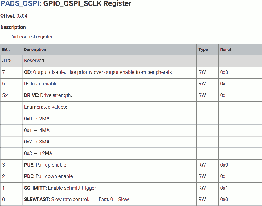
10000002:	4b32      	ldr	r3, =0x40020000	@ PADS_QSPI_BASE
10000004:	2021      	movs	r0, #0x21	@ 2 (8mA) << DRIVE | 1 << SLEWFAST
10000006:	6058      	str	r0, [r3, #4]	@ PADS_QSPI_BASE + GPIO_QSPI_SCLK
For the clock pin, use fast slew rate with 8mA drive strength.
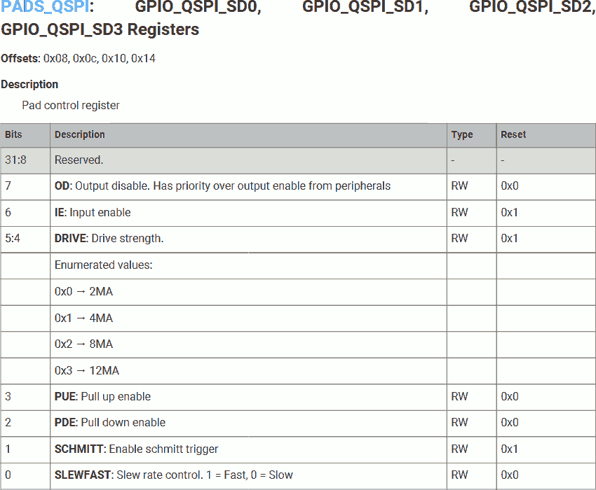
10000008:	6898      	ldr	r0, [r3, #8]	@ PADS_QSPI_BASE + GPIO_QSPI_SD0
1000000a:	2102      	movs	r1, #2		@ 1 << Schmitt
1000000c:	4388      	bics	r0, r1
1000000e:	6098      	str	r0, [r3, #8]	@ PADS_QSPI_BASE + GPIO_QSPI_SD0
10000010:	60d8      	str	r0, [r3, #12]	@ PADS_QSPI_BASE + GPIO_QSPI_SD1
10000012:	6118      	str	r0, [r3, #16]	@ PADS_QSPI_BASE + GPIO_QSPI_SD2
10000014:	6158      	str	r0, [r3, #20]	@ PADS_QSPI_BASE + GPIO_QSPI_SD3
For the all data pins, use the exsiting configuration (or default configuration), but disable the Schmitt triggers. This will increase the transfer rate, but less reliable signal.
Set SSI to Standard SPI
On power-up, the W25Q flash is in standrad SPI mode, we have to temporarily switch the SSI to standard SPI mode for flash configuration.
Set SSI BAUD Rate
10000016: 4b2e ldr r3, =0x18000000 @ XIP_SSI_BASE
10000018: 2100 movs r1, #0
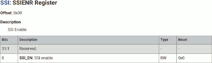
1000001a: 6099 str r1, [r3, #8] @ XIP_SSI_BASE + SSIENR
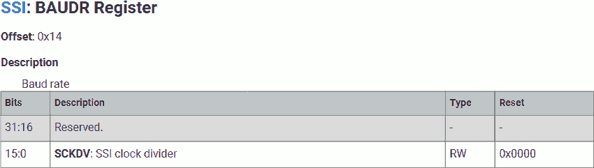
1000001c: 2102 movs r1, #2
1000001e: 6159 str r1, [r3, #20] @ XIP_SSI_BASE + BAUD
Disable SSI for configuration.
Set the SSI BAUD rate using clock divider of 2.
The value saved in r3 is the base address of XIP control registers, 0x18000000. Its value will never be modified in the 2nd stage bootloader. It is used in subsequent operations and subroutines.
Set SSI Sample Delay
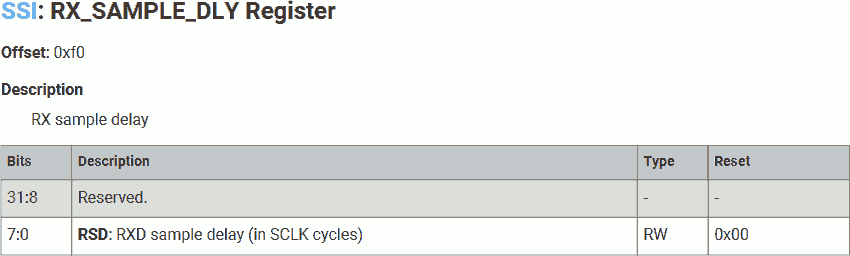
10000020:	2101      	movs	r1, #1
10000022:	22f0      	movs	r2, #0xf0
10000024:	5099      	str	r1, [r3, r2]	@ XIP_SSI_BASE + RX_SAMPLE_DLY
Set Rx delay to 1 clock cycle to compensate slow signal propagation speed.
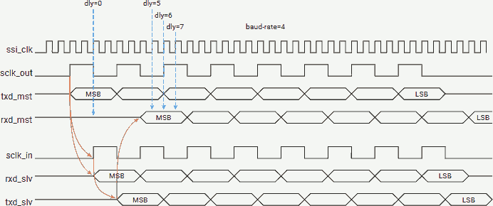
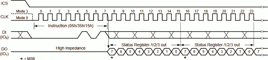
As the above figure show, there is signal propagation delay from master to slave, slave response delay, and signal propagation delay from slave to master.
Set SSI Mode
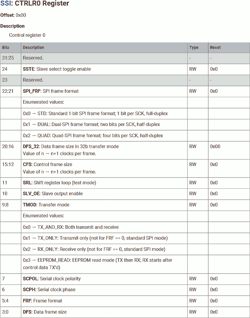
10000026:	492b      	ldr	r1, =0x00070000	@ 0 (STD) << SPI_FRF | 7 << DFS32 | 0 (TX_AND_RX) << TMOD
10000028:	6019      	str	r1, [r3, #0]	@ XIP_SSI_BASE + CTRLR0
1000002a:	2101      	movs	r1, #1
1000002c:	6099      	str	r1, [r3, #8]	@ XIP_SSI_BASE + SSIENR
Set the SSI mode:
SPI_FRF- 0 = Standard SPI.DFS_32- 7 = 8-bit data frame.TMOD- 0 = Enable both transmit and receive.
Re-enable SSI.
Flash Initialization
Before we can use W25Q in QSPI mode, we need to ensure it is ready to do so. If not, we will configurate it.
Check Flash Mode
1000002e:	2035      	movs	r0, #53
10000030:	f000 f844 	bl	ssi_writeread
10000034:	2202      	movs	r2, #2
10000036:	4290      	cmp	r0, r2
10000038:	d014      	beq.n	set_qspi
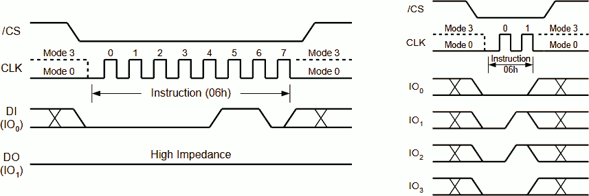
Sending 53 (0x35) to W25Q80 flash reads the status register 2. To send a word and receive a word, call subroutine ssi_writeread, see Subroutine - SSI Send and Receive 1 Word.
We expect response 2 (0b00000010), which means:
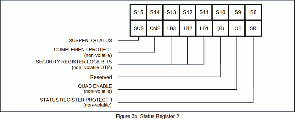
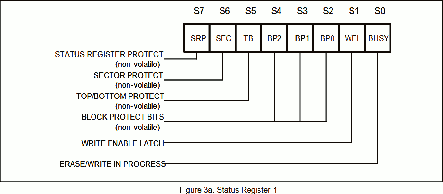
SUS= 0b0 - The flash program / earse is not suspended.CMP= 0b0 - Complement the protection area set bySEC,TBandBP. The W25Q flash allows write protection on top/bottom sectors. Since we are not using the protection function, we expect the default value 0.LB= 0b000 - Security register lock. The W25Q flash has 3 special 256-byte memory regions that can be locked once the security register lock bits are burned. It can be used to store one-time program data such as serial number. Since we are not using the security register, we expect the default value 0.QE= 0b1 - Quad IO (QSPI) enabled.SRL= 0b0 - Status register unlocked. The W25Q flash allows lock the status register until power cycle.
If true, flash is ready to be used in QSPI mode, skip to set_qspi, see Set SSI to QSPI. Otherwise, continue to initial the flash device.
Depending on order, the W25Q flash may be factory QSPI enabled.
Note these bits are non-volatile. The status remains unchanged after power cycle.
Therefore, we will be jump to set_qspi in most cases.
Enable Flash Write
1000003a:	2106      	movs	r1, #6
1000003c:	6619      	str	r1, [r3, #96]	@ XIP_SSI_BASE + DR0
1000003e:	f000 f834 	bl	ssi_waitsend
10000042:	6e19      	ldr	r1, [r3, #96]
We will need to enable write on the W25Q flash before we cam make any change. To do so, send 6 (0x06).
To send a word, write it into the Tx FIFO. Wait the send finished by calling subroutine ssi_waitsend, see Subroutine - Waiting SSI Sending.
Because SPI is 2-way synchronous, the master receiver samples the data input at the same time when the master transmitter sends, even the slave is not driving the SPI bus. Although the received word is a dummy, we need to read it to release it from the Rx FIFO.
Set Flash Mode
10000044:	2101      	movs	r1, #1
10000046:	6619      	str	r1, [r3, #96]	@ XIP_SSI_BASE + DR0
10000048:	2000      	movs	r0, #0
1000004a:	6618      	str	r0, [r3, #96]
1000004c:	661a      	str	r2, [r3, #96]
1000004e:	f000 f82c 	bl	ssi_waitsend
10000052:	6e19      	ldr	r1, [r3, #96]
10000054:	6e19      	ldr	r1, [r3, #96]
10000056:	6e19      	ldr	r1, [r3, #96]
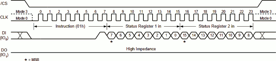
Sending 1 (0x01) to W25Q80 flash write the status register 1. If 2 bytes supplied, the status register 2 will be written as well. We will write 0 (0b00000000, saved in r0, set at program address 0x10000048) to status register registers 1, 2 (0b00000010, saved in r2, set at program address 0x10000034) to status register registers 2:
SRP= 0b0 - Use software protection. On W25Q flash, pin 3 can be used as write protection (hardware protection) or data IO 2.SEC= 0bx - Sector or block protect forBP. Not used in our application.TB= 0bx - Top or bottom protect forBP. Not used in our application.BP= 0b000 - Do not use block protect.WEL= 0bx - Write enable. Read-only, set by write enable instruction.BUSY= 0bx - The flash is busy for program / earse. Read-only.SUS= 0bx - The flash program / earse is suspended. Read-only.CMP= 0bx - Complement the protection area set bySEC,TBandBP. Not used in our application.LB= 0b000 - Do not use security register lock. (May be one-time programmable)QE= 0b1 - Enable quad IO (QSPI).SRL= 0b0 - Do not protect status register.
Wait the send finished by calling subroutine ssi_waitsend, see Subroutine - Waiting SSI Sending. Then, discard the returned dummy words.
Wait Flash Mode Set Finished
check_flash_busy:
10000058:	2005      	movs	r0, #5
1000005a:	f000 f82f 	bl	ssi_writeread
1000005e:	2101      	movs	r1, #1
10000060:	4208      	tst	r0, r1
10000062:	d1f9      	bne.n	check_flash_busy
Sending 5 (0x05) to W25Q80 flash reads the status register 1. To send a byte and receive a byte, call subroutine ssi_writeread, see Subroutine - SSI Send and Receive 1 Word.
Continuously polling the W25Q flash status register 1 until its value is 1 (0b00000001), which means:
SRP= 0b0 - Use software protection.SEC= 0b0 - Block protect forBP. Since we are not using the protection function, we expect the default value 0.TB= 0b0 - Top protect forBP. Since we are not using the protection function, we expect the default value 0.BP= 0b000 - No block protect.WEL= 0b1 - Write enabled.BUSY= 0b0 - The flash is not busy for program / earse.
Set SSI to QSPI
Once the W25Q flash is ready, we can switch SSI to QSPI mode.
Set SSI Mode
set_qspi:
10000064:	2100      	movs	r1, #0
10000066:	6099      	str	r1, [r3, #8]	@ XIP_SSI_BASE + SSIENR
10000068:	491b      	ldr	r1, =0x005f0300	@ 2 (QUAD) << SPI_FRF | 31 << DFS_32 | 3 (EEPROM_READ) << TMOD
1000006a:	6019      	str	r1, [r3, #0]	@ XIP_SSI_BASE + CTRLR0
Disable SSI for configuration.
Set the SSI mode:
SPI_FRF- 2 = QSPI. (Value used in next configuration)DFS_32- 31 = 32-bit data frame.TMOD- 3 = Use EEPROM_READ mode. The hardware use internal logic designed for EEPROM read.
Set SSI Data Size
1000006c: 2100 movs r1, #0
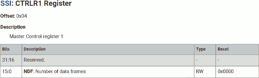
1000006e: 6059 str r1, [r3, #4] @ XIP_SSI_BASE + CTRLR1
Set data size to 0 words, for now. Basically, this means we are not expecting any data returned from the flash.
Note that, unlike standard mode, where sending and receiving happen simultaneously on two wires; in QSPI mode, the SSI is in half-duplex mode. The SSI will send data using all data wires first, then release the data bus(, but still drive the clock signal), then receive data from the slave.
After setting the data size to 0, the SSI will stop the data transmission immediately after sending data. Therefore, no data is returned from the salve.
Set SSI SPI Mode
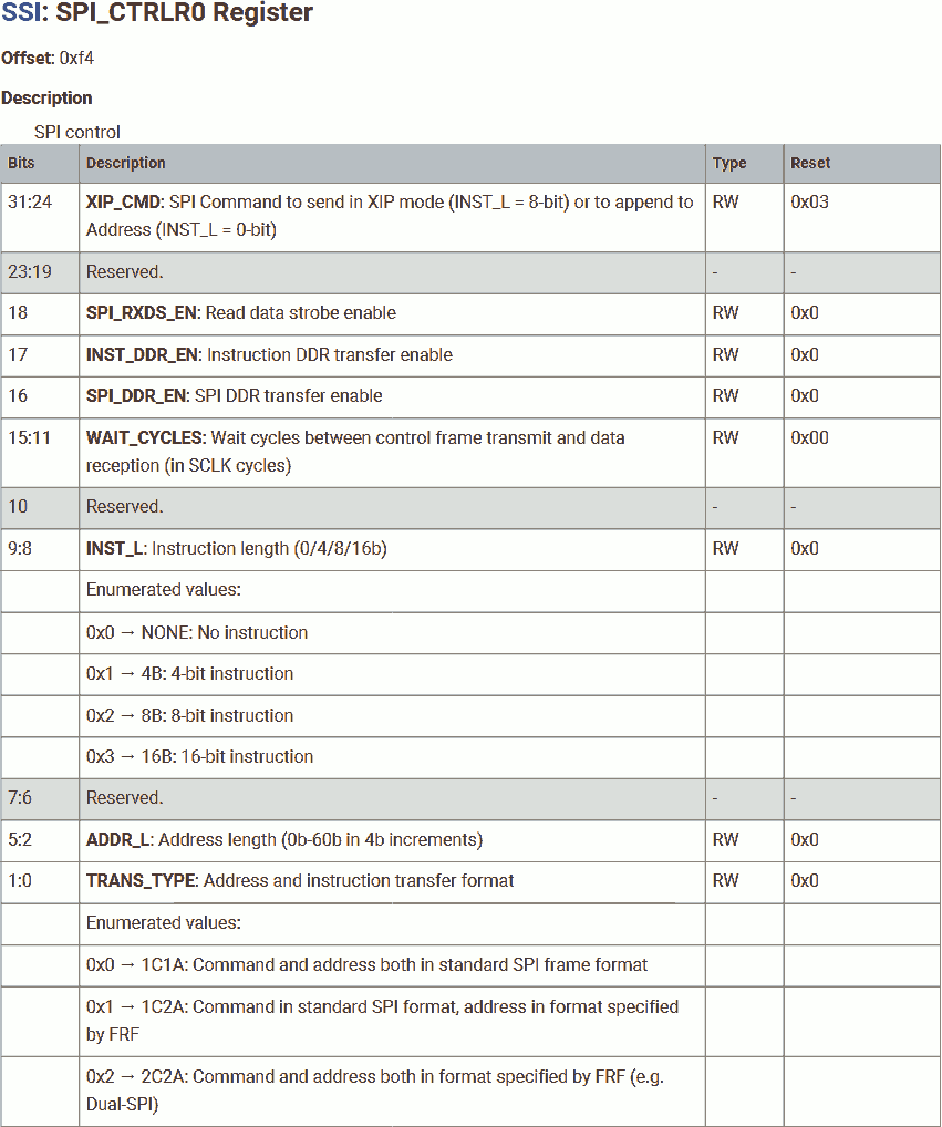
10000070:	491a      	ldr	r1, =0x00002221	@ 4 << WAIT_CYCLES | 2 (8B) << INST_L | 8 (x4) << ADDR_L | 1 (1C2A) << TRANS_TYPE
10000072:	481b      	ldr	r0, =0x180000f4	@ XIP_SSI_BASE + SPI_CTRLR0
10000074:	6001      	str	r1, [r0, #0]
10000076:	2101      	movs	r1, #1
10000078:	6099      	str	r1, [r3, #8]	@ XIP_SSI_BASE + SSIENR
Set the SSI SPI mode, according to the flash timing:
WAIT_CYCLES- 4 = Wait 4 cycles between sending and receiving. This gives the flash device to process the instruction, decode the address, switch IO and fetch the data.INST_L- 2 = 8-bit instruction.ADDR_L- 8 = 32-bit address.TRANS_TYPE- 1 = Send command (instruction) in SPI mode, but address in the mode specified byFRF(QSPI).
Re-enable SSI.
XIP Configuration
Set the flash and SSI in XIP mode.
Set Flash Read Mode
1000007a:	21eb      	movs	r1, #235
1000007c:	6619      	str	r1, [r3, #96]	@ XIP_SSI_BASE + DR0
1000007e:	21a0      	movs	r1, #160
10000080:	6619      	str	r1, [r3, #96]
10000082:	f000 f812 	bl	ssi_waitsend
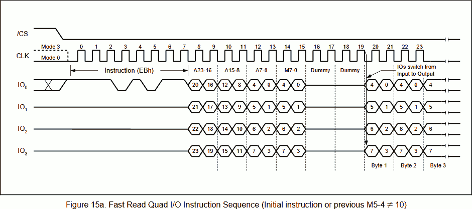
To read data from the W25Q80 flash using QSPI, send 8-bit instruction 0xEB, followed by 32-bit address.
The first 24 bits in the address frame (A23-A0) represent the actual data address, the last 8 bits in the address frame represent the continuation code. For this model (W25Q80EW), if the 5-th and 4-th (0-th is LSB) bits in the continuation code is not 0b10, the flash will enter the continuation mode. That means, in the next transaction, the instruction can be ignored. This reduces the overhead for sending the instruction in subsequent transactions.
We will send 32-bit address 160, that is 24-bit actual address 0x000000, followed by 8-bit continuation code 0b10100000.
Wait the send finished by calling subroutine ssi_waitsend, see Subroutine - Waiting SSI Sending. Then, discard the returned dummy words.
Set SSI SPI Mode
10000086:	2100      	movs	r1, #0
10000088:	6099      	str	r1, [r3, #8]	@ XIP_SSI_BASE + SSIENR
1000008a:	4916      	ldr	r1, =0xa0002022	@ 0xA0 << XIP_CMD | 4 << WAIT_CYCLES | 0 (0B) << INST_L | 8 (x4) << ADDR_L | 2 (2C2A) << TRANS_TYPE
1000008c:	4814      	ldr	r0, =0x180000f4	@ XIP_SSI_BASE + SPI_CTRLR0
1000008e:	6001      	str	r1, [r0, #0]
10000090:	2101      	movs	r1, #1
10000092:	6099      	str	r1, [r3, #8]	@ XIP_SSI_BASE + SSIENR
Disable SSI for configuration.
Set the SSI SPI mode, according to the flash timing:
XIP_CMD- 0xA0 = Continuation code appended after address.WAIT_CYCLES- 4 = Wait 4 cycles between sending and receiving.INST_L- 0 = No instruction, use continuation code instead.ADDR_L- 8 = 32-bit address.TRANS_TYPE- 2 = Send command (instruction) and data in the mode specified byFRF(QSPI).
Re-enable SSI.
Enter the Main Program
Determine Caller
10000094:	bc01      	pop	{r0}
10000096:	2800      	cmp	r0, #0
10000098:	d000      	beq.n	boot_launch
1000009a:	4700      	bx	r0
boot_launch:
Determine the caller of the bootloader, using the caller's address we saved at the first line of the 2nd stage bootloader. If the value is:
- Zero - A program called the 2nd stage bootloader: return to that program.
- Non-zero - The on-chip bootloader passed the control to the 2nd stage bootloader: Load the main program.
Vector Table
1000009c: 4812 ldr r0, =0x10000100
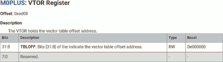
1000009e: 4913 ldr r1, =0xe000ed08 @ PPB_BASE + VTOR
100000a0: 6008 str r0, [r1, #0]
100000a2: c803 ldmia r0, {r0, r1} @ r0 <= [r0, #0], r1 <= [r0, #4]
100000a4: f380 8808 msr MSP, r0
100000a8: 4708 bx r1
Write the address of the vector table into the corresponding CPU register. In this program, we assume the vector table is placed immediately after the 2nd stage bootloader. Note the address of vector tabele must be aligned by 256 bytes.
The first vector (vector table address + 0) is the initial stack address. We will load it into MSP (main stack pointer).
The second vector (vector table address + 4) is the reset vector, which is the entry point of the mian program. We will bx (branch and exchange) to this address.
Subroutine
Subroutine - Waiting SSI Sending
ssi_waitsend:
100000aa: b503 push {r0, r1, lr}
ssi_waitsend_loop:
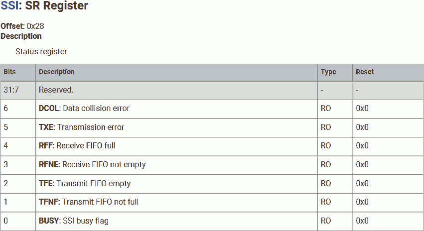
100000ac: 6a99 ldr r1, [r3, #40] @ XIP_SSI_BASE + SR
100000ae: 2004 movs r0, #4 @ 1 << TFE
100000b0: 4201 tst r1, r0
100000b2: d0fb beq.n ssi_waitsend_loop
100000b4: 2001 movs r0, #1 @ 1 << BUSY
100000b6: 4201 tst r1, r0
100000b8: d1f8 bne.n ssi_waitsend_loop
100000ba: bd03 pop {r0, r1, pc}
First of all, push all registers used in this subroutine into the stack to preserve their value. The caller does not expect their value to be changed.
Continuously poll the SSI status register until TFE and BUSY bits are cleared, which means:
TFE= 0b1 - Transmit FIFO is empty.BUSY= 0b0 - SSI is not busy.
Since SPI is a 2-way synchronous transmission protocol. Data sending and receiving finished simoustanly.
Restore used registers and return.
Subroutine - SSI Send and Receive 1 Word
ssi_writeread:
100000bc: b502 push {r1, lr}
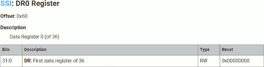
100000be: 6618 str r0, [r3, #96] @ XIP_SSI_BASE + DR0
100000c0: 6618 str r0, [r3, #96]
100000c2: f7ff fff2 bl ssi_waitsend
100000c6: 6e18 ldr r0, [r3, #96]
100000c8: 6e18 ldr r0, [r3, #96]
100000ca: bd02 pop {r1, pc}
First of all, push all registers used in this subroutine into the stack to preserve their value. The caller does not expect their value to be changed.
Data to send is passed in r0. we will send this 1-word data by writing it into the Tx FIFO. This data is used to command the salve. Because SPI is 2-way synchronous, the master receiver samples 1 word at the same time. At this moment, the slave is not driving the SPI bus, the sampled data is a dummy.
Send the 1-word data again. This is to drive the SPI clock to allow the slave to return data, the sending data will be ignored by the slave.
Once 2 words are sent, 2 words are available in the Rx FIOF. Although the first byte is a dummy, we need to read it into r0 to release it from the FIFO. The second word in the Rx FIFO is the actual data, read int into r0 to overwrite the last read dummy.
The SSI_DR0 register represents the top of the Tx and Rx FIFO. We can directly write and read this register to append and shift out the data. Internal pointers will coordinate the actual write and read address when data is appended or removed by read/write the FIFO register and sending/receiving by SSI hardware.
Restore used registers and return.
Constants Table
100000cc:	0000 4002
100000d0:	0000 1800
100000d4:	0000 0007
100000d8:	0300 005f
100000dc:	2221 0000
100000e0:	00f4 1800
100000e4:	2022 a000
100000e8:	0100 1000
100000ec:	ed08 e000
The Thumb instruction is 16-bit long. For the ldr (load immediate instruction), only 5 bits are used for the immediate value. This is definitely not enough for loading 32-bit constants.
Instead, we will need to store the 32-bit constants in program memory, then use ldr rd, pc+offset, that is, use the program counter as a read pointer with an offset. The constant must be stored near the ldr instruction due to the limit of offset.
Above are the constants used in the 2nd stage bootloader.
Custom C Program with SDK Bootloader
Create the SDK Bootloader
Now, let's put everything in the SDK bootloader together:
.cpu cortex-m0plus
.thumb
.align 2
.section .boot2, "ax"

boot2:
	push	{lr}

@ Pad setup
	ldr	r3, =0x40020000	@ PADS_QSPI_BASE
	movs	r0, #0x21	@ 2 (8mA) << DRIVE | 1 << SLEWFAST
	str	r0, [r3, #4]	@ PADS_QSPI_BASE + GPIO_QSPI_SCLK
	ldr	r0, [r3, #8]	@ PADS_QSPI_BASE + GPIO_QSPI_SD0
	movs	r1, #2		@ 1 << Schmitt
	bic	r0, r1
	str	r0, [r3, #8]	@ PADS_QSPI_BASE + GPIO_QSPI_SD0
	str	r0, [r3, #12]	@ PADS_QSPI_BASE + GPIO_QSPI_SD1
	str	r0, [r3, #16]	@ PADS_QSPI_BASE + GPIO_QSPI_SD2
	str	r0, [r3, #20]	@ PADS_QSPI_BASE + GPIO_QSPI_SD3

@ Use standard SPI for
	ldr	r3, =0x18000000	@ XIP_SSI_BASE
	movs	r1, #0
	str	r1, [r3, #8]	@ XIP_SSI_BASE + SSIENR
	movs	r1, #2
	str	r1, [r3, #20]	@ XIP_SSI_BASE + BAUD
	movs	r1, #1
	movs	r2, #0xf0
	str	r1, [r3, r2]	@ XIP_SSI_BASE + RX_SAMPLE_DLY
	ldr	r1, =0x00070000	@ 0 (STD) << SPI_FRF | 7 << DFS32 | 0 (TX_AND_RX) << TMOD
	str	r1, [r3, #0]	@ XIP_SSI_BASE + CTRLR0
	movs	r1, #1
	str	r1, [r3, #8]	@ XIP_SSI_BASE + SSIENR

@ Check flash in QSPI mode
	movs	r0, #53
	bl	ssi_writeread
	movs	r2, #2
	cmp	r0, r2
	beq	set_qspi

@ Enable falsh write
	movs	r1, #6
	str	r1, [r3, #96]	@ XIP_SSI_BASE + DR0
	bl	ssi_waitsend
	ldr	r1, [r3, #96]

@ Setup flash QSPI mode
	movs	r1, #1
	str	r1, [r3, #96]	@ XIP_SSI_BASE + DR0
	movs	r0, #0
	str	r0, [r3, #96]
	str	r2, [r3, #96]
	bl	ssi_waitsend
	ldr	r1, [r3, #96]
	ldr	r1, [r3, #96]
	ldr	r1, [r3, #96]

@ Wait flash ready
check_flash_busy:
	movs	r0, #5
	bl	ssi_writeread
	movs	r1, #1
	tst	r0, r1
	bne	check_flash_busy

@ Use QSPI and send fast read command to flash
set_qspi:
	movs	r1, #0
	str	r1, [r3, #8]	@ XIP_SSI_BASE + SSIENR
	ldr	r1, =0x005f0300	@ 2 (QUAD) << SPI_FRF | 31 << DFS_32 | 3 (EEPROM_READ) << TMOD
	str	r1, [r3, #0]	@ XIP_SSI_BASE + CTRLR0
	movs	r1, #0
	str	r1, [r3, #4]	@ XIP_SSI_BASE + CTRLR1
	ldr	r1, =0x00002221	@ 4 << WAIT_CYCLES | 2 (8B) << INST_L | 8 (x4) << ADDR_L | 1 (1C2A) << TRANS_TYPE
	ldr	r0, =0x180000f4	@ XIP_SSI_BASE + SPI_CTRLR0
	str	r1, [r0, #0]
	movs	r1, #1
	str	r1, [r3, #8]	@ XIP_SSI_BASE + SSIENR

@ Setup insturction bypass
	movs	r1, #235
	str	r1, [r3, #96]	@ XIP_SSI_BASE + DR0
	movs	r1, #160
	str	r1, [r3, #96]
	bl	ssi_waitsend

@ Setup QSPI with insturction bypass
	movs	r1, #0
	str	r1, [r3, #8]	@ XIP_SSI_BASE + SSIENR
	ldr	r1, =0xa0002022	@ 0xA0 << XIP_CMD | 4 << WAIT_CYCLES | 0 (0B) << INST_L | 8 (x4) << ADDR_L | 2 (2C2A) << TRANS_TYPE
	ldr	r0, =0x180000f4	@ XIP_SSI_BASE + SPI_CTRLR0
	str	r1, [r0, #0]
	movs	r1, #1
	str	r1, [r3, #8]	@ XIP_SSI_BASE + SSIENR

@ Exit 2nd stage bootloader
	pop	{r0}
	cmp	r0, #0
	beq	boot_launch
	bx	r0
	boot_launch:
	ldr	r0, =0x10000100
	ldr	r1, =0xe000ed08	@ PPB_BASE + VTOR
	str	r0, [r1, #0]
	ldmia	r0, {r0, r1}	@ r0 <= [r0, #0], r1 <= [r0, #4]
	msr	MSP, r0
	bx	r1

@ Wait SPI sent
ssi_waitsend:
	push	{r0, r1, lr}
ssi_waitsend_loop:
	ldr	r1, [r3, #40]	@ XIP_SSI_BASE + SR
	movs	r0, #4		@ 1 << TFE
	tst	r1, r0
	beq	ssi_waitsend_loop
	movs	r0, #1		@ 1 << BUSY
	tst	r1, r0
	bne	ssi_waitsend_loop
	pop	{r0, r1, pc}

@ SPI send 1 command and receive 1 data
ssi_writeread:
	push	{r1, lr}
	str	r0, [r3, #96]	@ XIP_SSI_BASE + DR0
	str	r0, [r3, #96]
	bl	ssi_waitsend
	ldr	r0, [r3, #96]
	ldr	r0, [r3, #96]
	pop	{r1, pc}
With the same linker script we used earlier, in file boot2_src.ld:
MEMORY {
	BOOT2(rx) : ORIGIN = 0x10000000, LENGTH = 256
}

SECTIONS {
	. = ORIGIN(BOOT2);
	.text : {
		KEEP(*(.boot2))
	} >BOOT2
}
Assemble, link, add checksum, the result is saved in file boot2.o:
arm-none-eabi-as --warn --fatal-warnings -g boot2_src.s -o boot2_src.o
arm-none-eabi-ld -nostdlib -nostartfiles -T boot2_src.ld boot2_src.o -o boot2_src.elf

arm-none-eabi-objcopy -O binary boot2_src.elf boot2_src.bin
pico-pad_checksum -s 0xFFFFFFFF boot2_src.bin boot2.s
arm-none-eabi-as --warn --fatal-warnings -g boot2.s -o boot2.o
The 2nd stage bootloader is now ready. Note that:
- XIP is used.
- The vector table must be saved at address 0x10000100, which is immediately after the 2nd stage bootloader.
- Checksum appended.
- When link, the section name is
boot2.
We can use the SDK 2nd stage bootloader object file boot2.o in other projects.
Main Program
Let's create the same blink program we used in my previous article; however, we will write it in C language this time, and save it in file main.c:
#include <stdint.h>

void reset();

uint32_t vector[48] __attribute__ ((section (".vector"))) = {
	0x20042000,
	(uint32_t)reset
};

void reset() {
	*(uint32_t volatile * const)(0x4000f000) = (1<<5);
	*(uint32_t volatile * const)(0x400140cc) = 5;
	*(uint32_t volatile * const)(0xd0000020) = (1<<25);

	for (;;) {
		*(uint32_t volatile * const)(0xd000001c) = (1<<25);
		for (uint32_t i = 30000; i; i--) { __asm("nop\n\t"); }
	}
}
At the beginning, we will need to define the vector table (a set of address):
- The first vector is the initial SP. In this program, we would like to use SRAM bank 5 (0x20041000 - 0x20041FFF) for stack; therefore, write the top address + 1 to this vector.
- The second vector is the entry point of the main program. We put the symbol
resethere. When link, the linker will place the address of the functionreset. - In this program, we don't worry about other vectors. Leave them undefined.
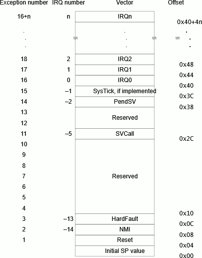
The RP2040 document states the Cortex-M0+ CPU has 34 WIC (Wake-up Interrupt Controller) lines (32 IRQ and NMI, RXEV). Which means, 16 + 32 = 48 vectors.
Name this vector table .vector, so we can access it during linking.
We had discussed the MCU control register addresses in previous article. The special *(uint32_t volatile * const)(0x4000f000) = data syntax can be used to write data directly to that address.
Compile this program against Cortex-M0+ CPU, use:
arm-none-eabi-gcc -mcpu=cortex-m0plus -c -O3 main.c -o main.o
Note we add the -c flag, this tells GCC to only compile the code, but don't link it. Otherwise, GCC will:
- Compile and link the program. GCC will look for
mainfunction as entry point. - Includes libraries.
- Setup environment.
Since we are creating baremetal application, we don't want any library nor environment, and we want to link the program manually.
The result is saved in file main.o.
Link
Create linker script in file flash.ld:
MEMORY {
	FLASH(rx) : ORIGIN = 0x10000000, LENGTH = 2048k
	SRAM(rwx) : ORIGIN = 0x20000000, LENGTH = 264k
}

SECTIONS {
	.text : {
		. = ORIGIN(FLASH);
		KEEP(*(.boot2))
		KEEP(*(.vector))
		KEEP(*(.text))
	} >FLASH
}
In this linker script, we place the boot2 code (2nd stage bootloader with checksum) at the beginning of the flash region, as required by the on-chip bootloader.
Immediately after the boot2 is the vector table. In other words, the vector table will be placed at address 0x10000100.
After the vector table is the text, which contains our main program.
Link the program and create the uf2 file:
arm-none-eabi-ld -nostdlib -nostartfiles -T flash.ld boot2.o main.o -o flash.elf
pico-elf2uf2 flash.elf flash.uf2
The generated file flash.uf2 can be download to Pico now.
In my next article, we will discuss how to launch core 1 from core 0 in a dual-core baremetal application.