Raspberry Pi Pico (RP2040) SRAM and Flash Programming
Program the Pico (RP2040) from the perspective of an 8-bit MCU developer’s view, focus on details in SRAM and flash memory programming.
Paspberry Pi Pico, RP2040, Flash, uf2, Linker script, ARM, Assembly, Baremetal, Bootloader, MCU, XIP
--by Captdam @ Mar 2, 2026Index
I have been working with 8-bit MCUs like 8051 and AVR for a long time; but new to 32-bit MCU like the RP2040 MCU on Raspberry Pi Pico board. In this blog, I will record my first trial on Pico from the perspective of an 8-bit MCU developer's view. I will be focused on programming the on-chip run-time memory and off-chip flash memory.
I will be writing baremetal Assembly and C language applications that directly writing / reading the MCU registers instead of using libraries. This expose me to the actual system control registers, allowing me to understanst the full functionality of the MCU.
This article is intended for developers who are familiar with 8-bit MCUs and use Assembly and C language to develop bare metal applications, but new to 32-bit RP2040 and ARM Cortex-M0+.
Since we are creating bare metal applications, we will be directly writing to and reading from the MCU control registers. No library is used.
We will rely on the documents heavily. It includes all information we need about the MCU control registers.
Because of the RP2040 document updates, and for some reason they decided to redirect my links to the old document to the new document, I decided to create a copy of the current version (2025-02-20) on my server. You may obtain this document from the official link here (as 2026-02-10).
Difference Between 8-bit MCU and 32-bit MCU
Other than the data wdith difference, the memory architecture is different between them.
8-bit MCUs in Harvard Architecture
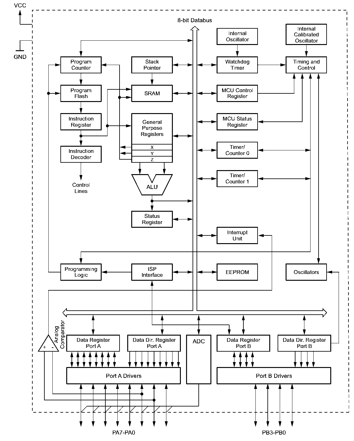
8-bit MCUs like 8051 and AVR are in Harvard architecture. The instruction (program) bus is connected to the program memory, the data bus is connected to the data memory. They are not crossed.
The program is saved on on-chip program memory, and in most cases, the on-chip flash. When we download the binary to MCU, we burn the program to the on-chip flash. When the MCU starts, the CPU execution unit directly reads the on-chip flash.
Other than the flash, there is the data memory. It can be an on-chip SRAM, or an external memory chip, or both. This memory is for data only, the CPU cannot execute from it.
32-bit MCUs in Von Neumann Architecture
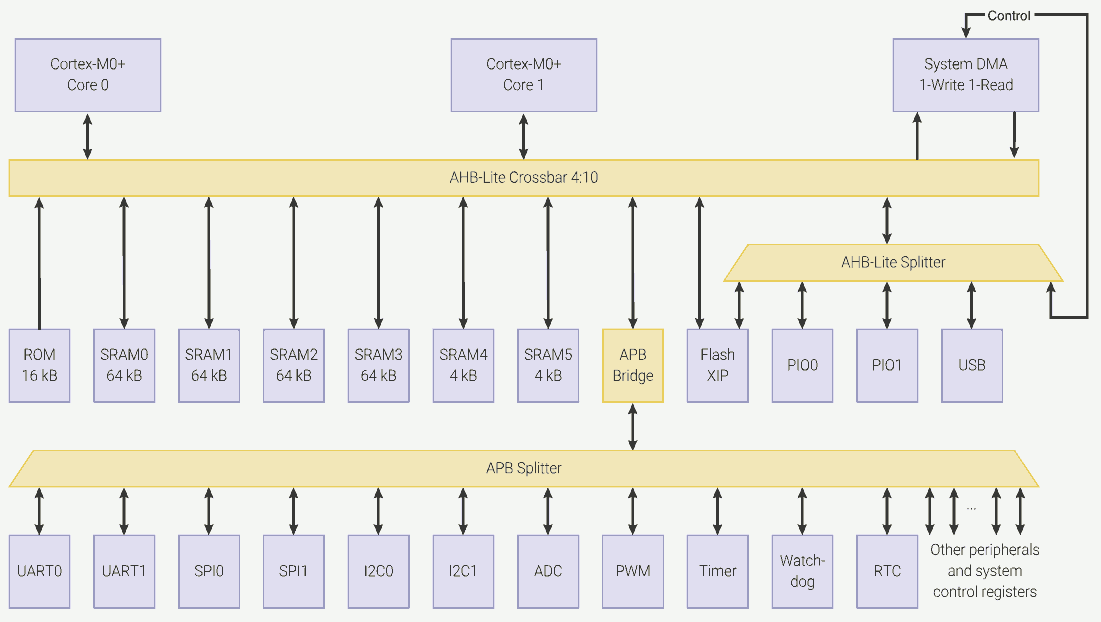
32-bit MCU like the RP2040 are in Von Neumann architecture. The instruction bus and the data bus are connected to the same memory. There is only one universal memory interface, for ARM architecture, that's the AHB-Lite Crossbar.
More specifically, one memory space. From the CPU's perspective, it only sees one memory space. Regions in the one universal memory space can be specialized, some allow write and read, some are read only; some can be used for data only, some can be used for program only, some can be used as both; and some are mapped to MCU control registers. The memory bus will map different physical memories into one memory space.
The CPU is connected to the mian memory, but not a flash that store program in a non-volatile way. To execute a program, a bootloader must load the program into a executable region in the main memory before the CPU can execute it.
RP2040 supports execution in place (XIP). It seems that the CPU can execute from off-chip flash (or any device connected to the QSPI port); however, the XIP hardware must first cache the program into the on-chip memory. Therefore, the CPU is executing the program in the on-chip memory.
HelloWorld.asm
We will write a very simple program that blinks the on-board LED on GPIO25.
Project file for this example can be found here.
ASM Program
Following is our program source code in assembly language in file main.s:
Architecture
.cpu cortex-m0plus
.thumb
.align 2
.thumb_func
At the beginning, we tell the assembler that we are using Cortex M0+ CPU (the CPU used by RP2040).
This CPU supports Thumb instruction set only, where the width of instruction is 2 bytes. Therefore, we let the assembler use the Thumb instruction set and we would like to align the instruction code by 2 bytes.
Entry Point
.global reset
reset:
	ldr	r0, =0x20041000		@ Stack Pointer @ SRAM bank 4
	mov	sp, r0
Our entry point is routine reset. We will make the label reset global. In that way, the reset routine will be visible in the linking stage.
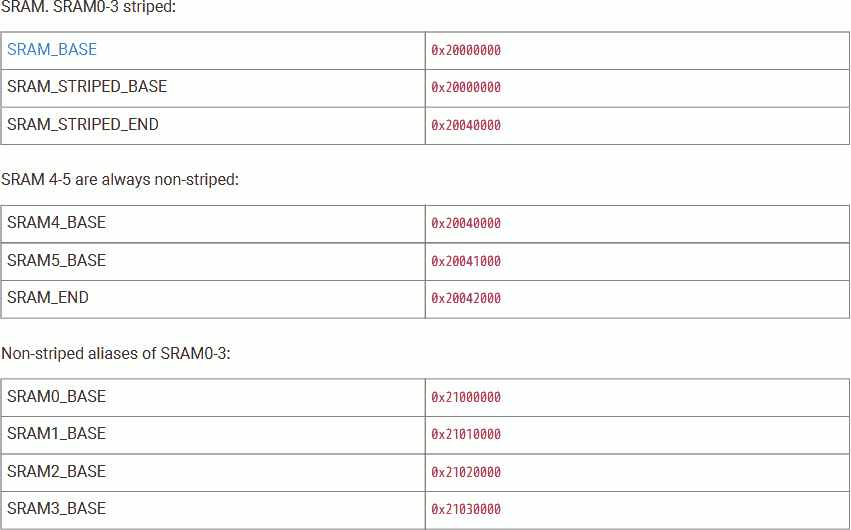
We want to use SRAM bank 4 (address 0x20004000 - 0x200040FFF, 4KiB in size) as our stack. The ARM Cortex-M0+ CPU stack pointer (SP) indicates the last stacked item on the stack memory and grows downwards; therefore, we need to set the initial SP at the top of the memory region + 1. That is, 0x20041000. Save this address into stack pointer SP.
Enable Output
	ldr	r3, =0x4000f000		@RESETS_BASE + RESET  + 0x3000
	mov	r2, #32			@ 1 << 5 (IO_BANK0)
	str	r2, [r3, #0]
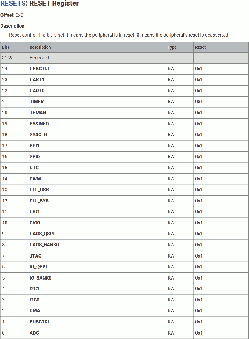
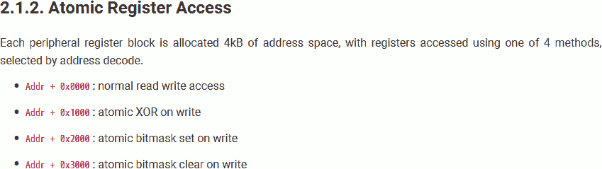
After power-up, the user IOs (IO Bank 0, GPIO 0 - 29) is in reset; hence, we need to bring it out of reset before use. To do so, we will need to clear the 5th bit (IO_BANK0) of the RESET register (address 0x4000C000).
Furthermore, adding an address offset of 0x3000 allows atomically write 1 to clear bits. Therefore, we will write (1<<5) to address 0x4000F000.
IO Mode
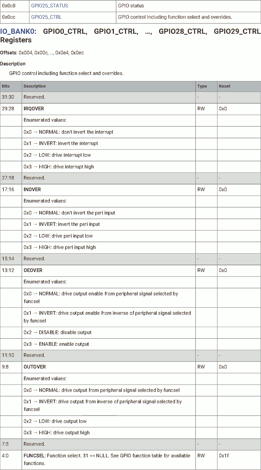
ldr r3, =0x400140cc @ IO_BANK0_BASE + GPIO25_CTRL
mov r2, #5 @ Function 5 (SIO)
str r2, [r3, #0]
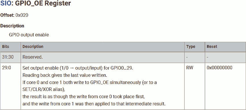
ldr r3, =0xd0000020 @ SIO_BASE + GPIO_OE
ldr r2, =(1<<25)
str r2, [r3, #0]
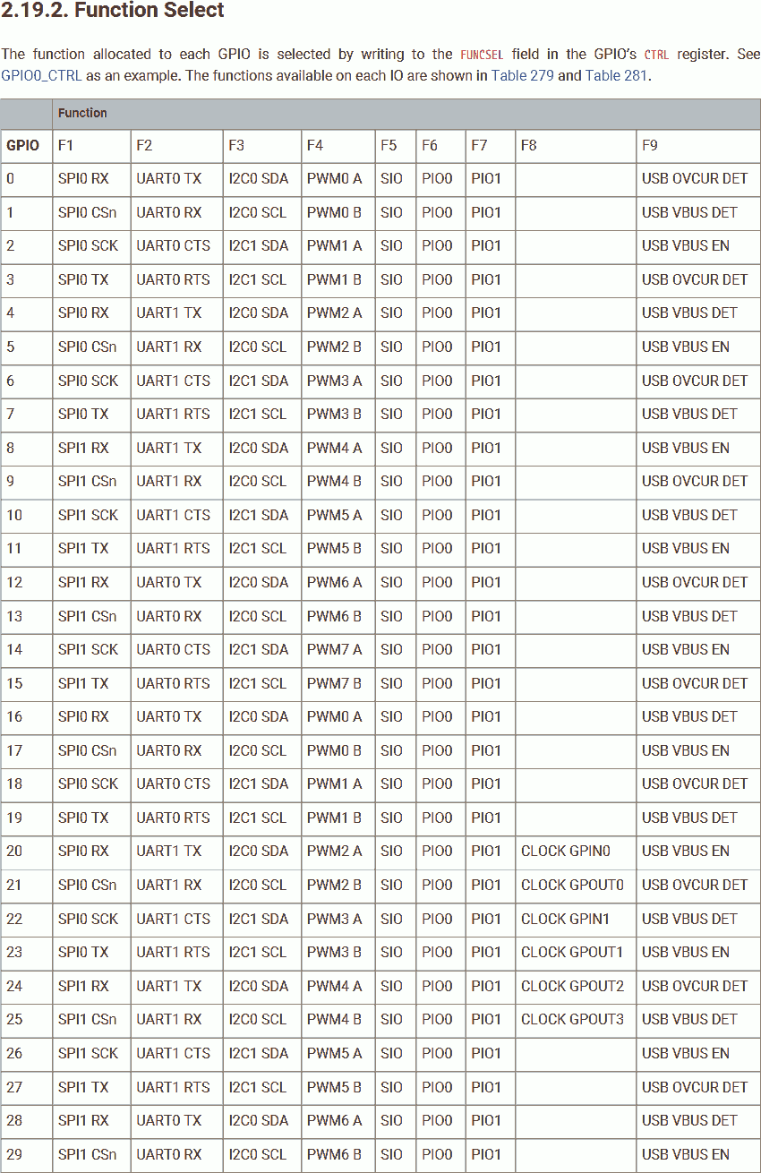
To set the functionality of GPIO25, we will need to write the functionality to address 0x400140CC (GPIO25_CTRL). To use it as a simple IO, write 5 (for SIO).
To use GPIO25 for output, write 1 to the 25th bit on register at address 0xD0000020 (GPIO_EN).
Blink
blink:
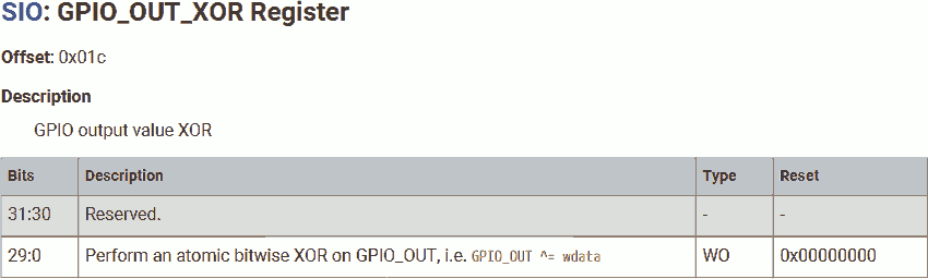
ldr r3, =0xd000001c @ SIO_BASE + GPIO_XOR
ldr r2, =(1<<25) @ GPIO25
str r2, [r3, #0]
ldr r0, =650000
bl delay
b blink
delay:
mov r4,r0
loop:
sub r4,r4,#1
cmp r4, #0
bne loop
bx lr
.align 4
The routine blink is used to blink the LED. To blink the LED on GPIO25, we will xor that bit. To atomically xor that bit, write 1 to 25th bit on register at address 0xD000001C (GPIO_OUT_XOR).
The routine delay is used to generate some busy-delay between each XOR operation using the loop under the label loop.
These labels / routines are used only in this file, and don't need to be visible in the linking stage; therefore, don't need to be global.
It is always a good idea to restore the default alignment of 4 for the 32-bit CPU at the end. This doesn't apply to Cortex-M0+ which uses Thumb instruction only, that is 2-byte aligned, but apply to other ARMs. Let's use it to stay safe.
To assemble this code, use arm-none-eabi-as --warn --fatal-warnings -g main.s -o main.o, result saved in file main.o.
Linker Script
Once assembled, we have to link the program to the target platform. Assembly only makes the program executable, linking makes it loadable.
Following is our linker script in file main.ld:
MEMORY {
	SRAM(rwx) : ORIGIN = 0x20000000, LENGTH = 264k
}

ENTRY(reset)

SECTIONS {
	. = ORIGIN(SRAM);
	.text : {
		*(.text)
	} >SRAM
}
In this linker script, we tell the linker:
- There is a readable and writeable memory called SRAM, starting at address 0x20000000, that is 264KiB long.
- Entry point is the routine
reset. Start execution from that position. - Put the text segment (program code) in SRAM, starting from the origin (beginning) of SRAM.
To link this program, use arm-none-eabi-ld -nostdlib -nostartfiles -T main.ld main.o -o main.elf, result saved in file main.elf
UF2 File
Now, the program is ready. To download it to the Pico, we will need to do one more step: pack it into uf2 format to download via USB.
The RP2040 provides a very easy-to-use way to download. Compared to the traditional method that requires a physical programmer (or a special interface not common on modern PCs such as UART), RP2040 supports download over USB. Once powered up, RP2040 will represent itself as a mass storage device. This allows the developer to download the program file the same way as copy a file into a USB disk.
To generate the uf2 file, use pico-elf2uf2 main.elf main.uf2, result saved in file main.uf2.
You can download the SDK source code but you will need to build the SDK to run it on your computer.
You can find the elf2uf2 program in pico-sdk/elf2uf2 (SDK version 1). See source code in /tools/elf2uf2 in SDK1.5.1 on GitHub.
I copied the elf2uf2 program into my environment /bin to use it directly.
We can open the uf2 file in hex mode to check its content, use od -t x4 main.uf2:
Addr    X0       X4       X8       XC
0000000 0a324655 9e5d5157 00002000 20000000
0000020 00000100 00000000 00000001 e48bff56
0000040 4685480b 22204b0b 4b0b601a 601a2205
0000060 4a0b4b0a 4b0b601a 601a4a09 f000480a
0000100 e7f8f801 3c011c04 d1fc2c00 46c04770
0000120 20041000 4000f000 400140cc d0000020
0000140 02000000 d000001c 0009eb10 00000000
0000160 00000000 00000000 00000000 00000000
*
0000760 00000000 00000000 00000000 0ab16f30
0001000
Cross reference the UF2 format, we can understant the content as follow:
| Offset,Size | Name | Content | Comment |
|---|---|---|---|
| 0,8 | Magic number: 0x0A324655, 0x9E5D5157 | 0a324655 9e5d5157 | |
| 8,4 | Flag | 00002000 | familyID present - when set, the fileSize/familyID holds a value identifying the board family (usually corresponds to an MCU) |
| 12,4 | Address in flash (memory for RP2040) where the data should be written | 20000000 | Same as the linker script ORIGIN(SRAM), beginning of SECTIONS |
| 16,4 | Number of bytes used in data (often 256) | 00000100 | 256 bytes long |
| 20,4 | Sequential block number; starts at 0 | 00000000 | 0, first block |
| 24,4 | Total number of blocks in file | 00000001 | 1 block only |
| 28,4 | File size or board family ID or zero | e48bff56 | Family ID for RP2040, see this list |
| 32,476 | Data, padded with zeros | 4685480b... | The program, verify with arm-none-eabi-objdump -d main.elf |
| 508,4 | Final magic number: 0x0AB16F30 | 0ab16f30 |
Download to Pico
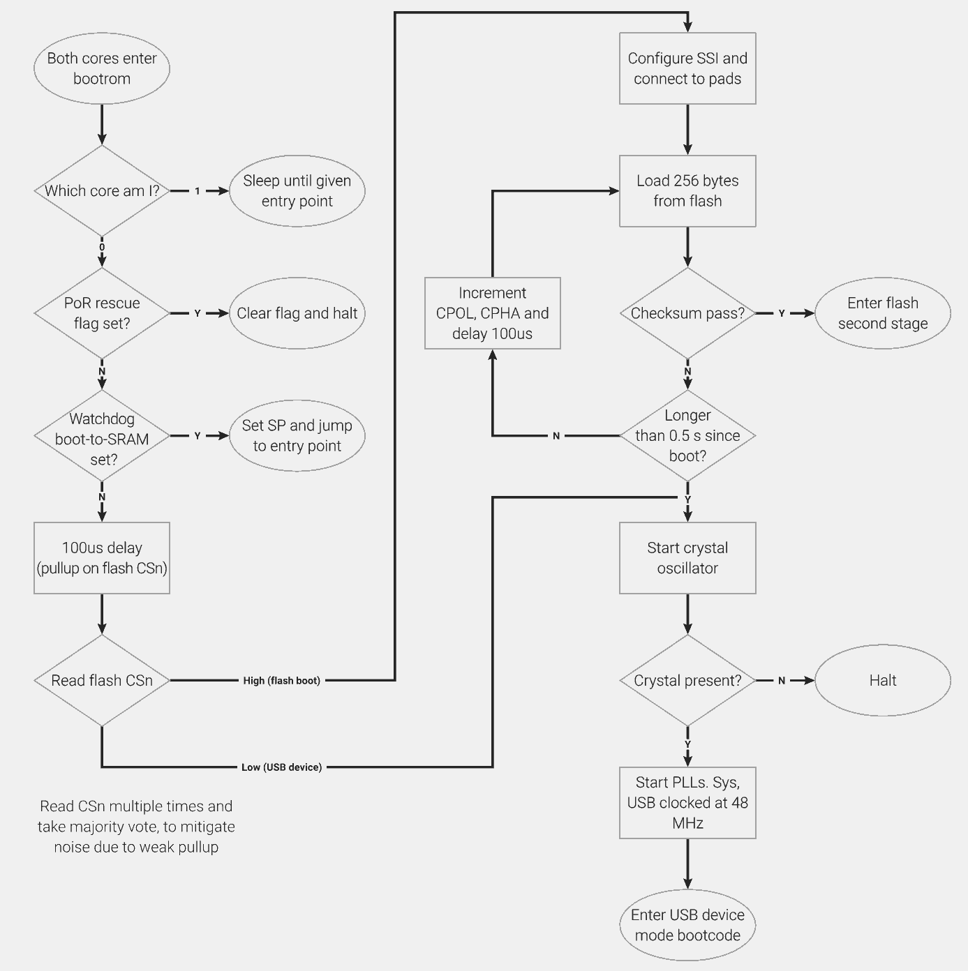
When we power the Pico up, the CPU starts executing the on-chip bootloader (offen called the first stage bootloader). This bootloader program is located at the boot ROM and cannot be changed. This bootloader allows the Pico to be connected to PC via USB as a mass storage device (like a USB disk) for programming.
RP2040 will start as a USB mass storage device if the BOOTSEL button pressed (connected to the on-board Flash CSn pin, RP2040 pin 56), or ther is no valid program in the Flash.
We can program the chip by copying the uf2 program file into the mass storage device.
Once the uf2 file is received, the bootloader will try to copy the content in that file into specified location.
We can see the LED on the Pico board blinking.
Download to SRAM vs to Flash
Cut the power, then connect the power. The program disappeared. The Pico starts as a mass storage device. Where the h... is my program?
Download to SRAM
In our linker script, we have:
MEMORY {
	SRAM(rwx) : ORIGIN = 0x20000000, LENGTH = 264k
}
This causes the uf2 file to use the 0x20000000 as target address. Therefore, the bootloader will copy the content of the uf2 file (which is our program) to address 0x20000000. For RP2040, this address is mapped to SRAM.
The SRAM is volatile. Once the power is lost, its content is lost.
In fact, even if the program is not lost in SRAM, the CPU will always stall in on-chip bootloader stage. It either waiting for new uf2 file if the flash is invalid, or reload the program from the flash if the flash is valid.
Download to Flash
According to the datasheet, the XIP address starts from 0x10000000. This address maps the external 2MiB on-board flash chip.
RP2040's flash address width allows a size of up to 16MiB (0x01000000). The flash is mirrored 4 times, spanning from 0x10000000 to 0x13FFFFFF, for different cache strategies. 0x10000000 - 0x10FFFFFF represents the most basic one, the “cacheable, allocating - Normal cache operation”. For the on-chip bootloader, writing to 0x10000000 - 0x10FFFFFF means write to the physical flash; writing to 0x11000000 - 0x13FFFFFF is not allowed.
To download to the XIP (flash) memory, we will need to link the program to that location in order to let the on-chip bootloader copy our program into the physical falsh.
Let's modify the liner script to write to 0x10000000, as follow:
MEMORY {
	Flash(rx) : ORIGIN = 0x10000000, LENGTH = 2048k
}

ENTRY(reset)

SECTIONS {
	. = ORIGIN(Flash);
	.text : {
		*(.text)
	} >Flash
}
Keep the assembly code source file untouched. Relink, regenerate the uf2 file, use arm-none-eabi-ld -nostdlib -nostartfiles -T main.ld main.o -o main.elf then pico-elf2uf2 main.elf main.uf2.
If we check the content of the newly generated uf2 file, we can find that the content at file offset 12 (Address in flash where the data should be written) changed to 0x10000000. This tells the on-chip bootloader to write the program to 0x10000000, which is mapped to the on-board flash.
Program the chip by copying the uf2 program file into the mass storage device. It failed. The LED is not blinking. The chip stalls at on-chip bootloader stage. Shortly after Pico received the uf2 file, it presents itself as a mass storage device again.
If there is a valid program in the flash, it will be overwritten.
The Checksum
From the CPU's perspective of view, there is no programmed, or un-programmed flash. Reading the flash always produces some result, either 1 or 0, ther is no such thing like "undefined". An un-programmed flash will provide random bytes, or all empty bytes (there is always some data).
At power up, the on-chip bootloader will read 256 bytes of data from the on-board flash. Then, it uses checksum to verify the data from the flash:
- If the checksum passed, the on-chip bootloader will treat the data as a valid program and start execution from it.
- If failed, the on-chip bootloader will treat the data as some random garbage. RP2040 will represent itself as a mass storage device, ready to receive new programs.
The reason is: We had the program in flash, but without a correct checksum. So, the on-chip bootloader failed to load our program.
Download to Flash
Now, we will be working on programming the flash, so the program can be preserved after power lost.
Project file for this example can be found here.
The Source Code
Before we add the checksum, we have to make a slight modification on our assembly source code:
.cpu cortex-m0plus
.thumb
.align 2
.thumb_func

.section .boot2, "ax"
.global reset
reset:
	ldr	r0, =0x20041000		@ Stack Pointer @ SRAM bank 4
	mov	sp, r0

	ldr	r3, =0x4000f000		@RESETS_BASE + RESET  + 0x3000
	mov	r2, #32			@ 1 << 5 (IO_BANK0)
	str	r2, [r3, #0]

	ldr	r3, =0x400140cc		@ IO_BANK0_BASE + GPIO25_CTRL
	mov	r2, #5			@ Function 5 (SIO)
	str	r2, [r3, #0]

	ldr	r3, =0xd0000020		@ SIO_BASE + GPIO_OE
	ldr	r2, =(1<<25)
	str	r2, [r3, #0]

blink:
	ldr	r3, =0xd000001c		@ SIO_BASE + GPIO_XOR
	ldr	r2, =(1<<25)	@ GPIO25
	str	r2, [r3, #0]

	ldr	r0, =650000
	bl	delay
	b	blink

delay:
	mov	r4,r0
loop:
	sub	r4,r4,#1
	cmp	r4, #0
	bne	loop
	bx	lr

.align 4
We add .section .boot2, “ax”. This is to name the following program code boot2, and indicate the program is allocatable and executable.
Save this source code as boot2_src.s.
Assemble it, use arm-none-eabi-as --warn --fatal-warnings -g boot2_src.s -o boot2_src.o, result saved in file boot2_src.o.
We also need some modification on the linker script:
MEMORY {
	FLASH(rx) : ORIGIN = 0x10000000, LENGTH = 2048k
	SRAM(rwx) : ORIGIN = 0x20000000, LENGTH = 264k
}

SECTIONS {
	. = ORIGIN(FLASH);
	.text : {
		KEEP(*(.boot2))
	} >FLASH
}
Store the boot2 section at the beginning of flash.
Save this linker script as boot2_src.ld.
Link it, use arm-none-eabi-ld -nostdlib -nostartfiles -T boot2_src.ld boot2_src.o -o boot2_src.elf, result saved in file boot2_src.elf.
Generate a binary file containing the program code, use arm-none-eabi-objcopy -O binary boot2_src.elf boot2_src.bin, result saved in file boot2_src.bin. We can check the content of this binary file using od -t x4 boot2_src.bin:
0000000 4685480b 22204b0b 4b0b601a 601a2205
0000020 4a0b4b0a 4b0b601a 601a4a09 f000480a
0000040 e7f8f801 3c011c04 d1fc2c00 46c04770
0000060 20041000 4000f000 400140cc d0000020
0000100 02000000 d000001c 0009eb10
0000114
To be honest, it is not necessary to neither name the section boot2 in source code nor specify the memories and sections in the linker script. They all got destroyed in the binary file.
However, it is a good idea to properly name and link them, so we don't get confused in the future.
Append the Checksum
The RP2040 document says, the on-chip bootloader will load the first 256 bytes from the flash into SRAM bank 5 and verify the checksum:
- Use CRC32.
- Polynomial: 0x04c11db7.
- Initial value: 0xffffffff.
We will add the checksum using the tool that comes with the SDK. Use pico-pad_checksum -s 0xFFFFFFFF boot2_src.bin boot2.s, result saved in boot2.s. We can open this assembly source code file in text mode:
// Padded and checksummed version of: boot2_src.bin

.cpu cortex-m0plus
.thumb

.section .boot2, "ax"

.byte 0x0b, 0x48, 0x85, 0x46, 0x0b, 0x4b, 0x20, 0x22, 0x1a, 0x60, 0x0b, 0x4b, 0x05, 0x22, 0x1a, 0x60
.byte 0x0a, 0x4b, 0x0b, 0x4a, 0x1a, 0x60, 0x0b, 0x4b, 0x09, 0x4a, 0x1a, 0x60, 0x0a, 0x48, 0x00, 0xf0
.byte 0x01, 0xf8, 0xf8, 0xe7, 0x04, 0x1c, 0x01, 0x3c, 0x00, 0x2c, 0xfc, 0xd1, 0x70, 0x47, 0xc0, 0x46
.byte 0x00, 0x10, 0x04, 0x20, 0x00, 0xf0, 0x00, 0x40, 0xcc, 0x40, 0x01, 0x40, 0x20, 0x00, 0x00, 0xd0
.byte 0x00, 0x00, 0x00, 0x02, 0x1c, 0x00, 0x00, 0xd0, 0x10, 0xeb, 0x09, 0x00, 0x00, 0x00, 0x00, 0x00
.byte 0x00, 0x00, 0x00, 0x00, 0x00, 0x00, 0x00, 0x00, 0x00, 0x00, 0x00, 0x00, 0x00, 0x00, 0x00, 0x00
.byte 0x00, 0x00, 0x00, 0x00, 0x00, 0x00, 0x00, 0x00, 0x00, 0x00, 0x00, 0x00, 0x00, 0x00, 0x00, 0x00
.byte 0x00, 0x00, 0x00, 0x00, 0x00, 0x00, 0x00, 0x00, 0x00, 0x00, 0x00, 0x00, 0x00, 0x00, 0x00, 0x00
.byte 0x00, 0x00, 0x00, 0x00, 0x00, 0x00, 0x00, 0x00, 0x00, 0x00, 0x00, 0x00, 0x00, 0x00, 0x00, 0x00
.byte 0x00, 0x00, 0x00, 0x00, 0x00, 0x00, 0x00, 0x00, 0x00, 0x00, 0x00, 0x00, 0x00, 0x00, 0x00, 0x00
.byte 0x00, 0x00, 0x00, 0x00, 0x00, 0x00, 0x00, 0x00, 0x00, 0x00, 0x00, 0x00, 0x00, 0x00, 0x00, 0x00
.byte 0x00, 0x00, 0x00, 0x00, 0x00, 0x00, 0x00, 0x00, 0x00, 0x00, 0x00, 0x00, 0x00, 0x00, 0x00, 0x00
.byte 0x00, 0x00, 0x00, 0x00, 0x00, 0x00, 0x00, 0x00, 0x00, 0x00, 0x00, 0x00, 0x00, 0x00, 0x00, 0x00
.byte 0x00, 0x00, 0x00, 0x00, 0x00, 0x00, 0x00, 0x00, 0x00, 0x00, 0x00, 0x00, 0x00, 0x00, 0x00, 0x00
.byte 0x00, 0x00, 0x00, 0x00, 0x00, 0x00, 0x00, 0x00, 0x00, 0x00, 0x00, 0x00, 0x00, 0x00, 0x00, 0x00
.byte 0x00, 0x00, 0x00, 0x00, 0x00, 0x00, 0x00, 0x00, 0x00, 0x00, 0x00, 0x00, 0xda, 0x37, 0x23, 0x75
As we can see, this file contains the program code (see file boot2_src.bin) plus 4 bytes of checksum at the end of the file. The total length is 256 bytes.
Note that at the top of this assembly code, they had been given the section name boot2. This is because in most cases, this code (the first 256 bytes read by on-chip bootloader) is used as the second stage bootloader, which loads the main program.
You can find the pad_checksum program in pico-sdk/src/rp2_common/boot_stage2 (SDK version 1). See source code in /src/rp2_common/boot_stage2 in SDK1.5.1 on GitHub.
I copied the pad_checksum program into my environment /bin to use it directly.
This tool is a Python script. By default, it uses 256 as pad size, 0 as seed (initial value). We are OK with 256 pad size, but we would like to change the initial value (seed) to 0xFFFFFFFF by using -s 0xFFFFFFFF.
Inside this tool, on line 42, there is ((binascii.crc32(bytes(bitrev(b, 8) for b in idata_padded), args.seed ^ 0xffffffff) ^ 0xffffffff) & 0xffffffff, 32). In the Python document, it states: binascii.crc32: Compute CRC-32, the unsigned 32-bit checksum of data, starting with an initial CRC of value. … The algorithm is consistent with the ZIP file checksum. According to GZIP File Format Specification, page 12, the polynomial in ZIP algorithm is 0xedb88320, which is the reverse of 0x04c11db7 required by RP2040 on-chip bootloader.
UF2 File with Checksum
Finally, we can download the program with proper checksum.
Assemble the padded and checksummed assembly code, use arm-none-eabi-as --warn --fatal-warnings -g boot2.s -o boot2.o, result saved in file boot2.o.
Create a new linker script:
MEMORY {
	FLASH(rx) : ORIGIN = 0x10000000, LENGTH = 2048k
	SRAM(rwx) : ORIGIN = 0x20000000, LENGTH = 264k
}

SECTIONS {
	. = ORIGIN(FLASH);
	.text : {
		KEEP(*(.boot2))
	} >FLASH
}
This will place the boot2 section (our program with checksum) at the beginning of the flash (mapped to XIP at address 0x10000000). This should request the on-chip bootloader to burn the program to flash after it received the uf2 file.
Link it, use arm-none-eabi-ld -nostdlib -nostartfiles -T main.ld boot2.o -o main.elf, result saved in file main.elf.
Generate uf2 file, use pico-elf2uf2 main.elf boot2.uf2, result saved in file boot2.uf2.
Program the chip. Remove the power and reapply the power.
Our program is kept.
The Next Step
As we can see, the on-chip bootloader will only load 256 bytes of data from flash (including 4 bytes of checksum), that is, only 126 Thumb instructions (2 bytes each). This is far less than the space to store a reasonable program.
Therefore, we have to introduce the second stage bootloader (boot2) that fits into the 256-byte space, saved in flash. Its only purpose is to prepare the main program execution.
In my next article, we will discuss the SDK 2nd stage bootloader.