My Go-to ATtinys
This blog will introduce ATtiny chips in DIP / SOIC packages and with SPI-based ICSP interface that I have been used in my projects.
AVR, ATtiny, Embedded system, ATtiny25, ATtiny24, ATtiny441, ATtiny261, ATtiny2313, ATtiny48
--by Captdam @ Aug 5, 2025Index
The AVR microprocessors can be divided into two categories: the light-weight ATtiny series, such as ATtiny25; and the powerful ATmega, such as ATmega328 seen on Arduino UNO. Generally speaking, ATtinys have less pins and less hardwares, and lack hardware multipliers in their ALU, but cost less. On the other hand, ATmegas have more pins, and come with a complete set of communication peripherals; hence can be used to implement a much more complex system; but with higher cost. It is worth to mentions that, both ATtinys and ATmegas have identical CPUs (except hardware multiplier) and run at the same speed. And for some chips with more than 64KB memory space (such as ATmega 2560), they require one extra clock to access the memory and to branch the program, so they are eventually slower.
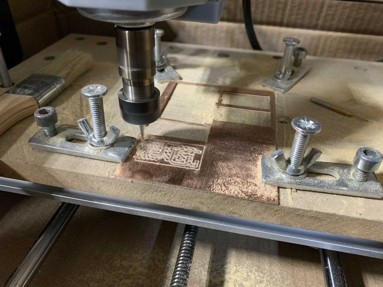
Because I create my PCB using the mechanical method, which is to use CNC to engrave circuit traces on copper-plated plates.I would prefer to make PCB in small size. It saves milling time and allows more error due to unlevel bed. However, because of the size of the milling bits, the minimum feature size my machine can make is 0.007-inch (0.2mm). In other words, I can only reliably make PCB for DIP package (2.54mm pitch) ICs or SOIC package (1.27mm pitch) ICs. For other components not requiring dense traces, my machine accepts smaller packages like SOT-23 used on 2N7002.
ATtiny25
ATtiny25 ATtiny45 ATtiny85
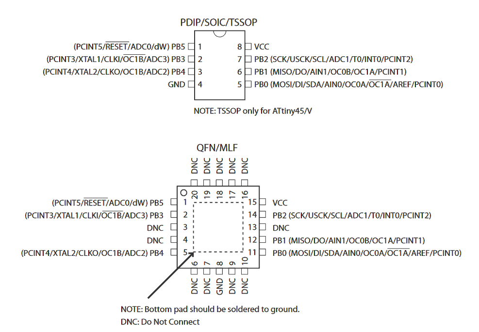
Highlights
Smallest, and most cost-saving AVR (we have ATtiny4 now, but requires TPI to program). It can be used to implement extremely small circuits.
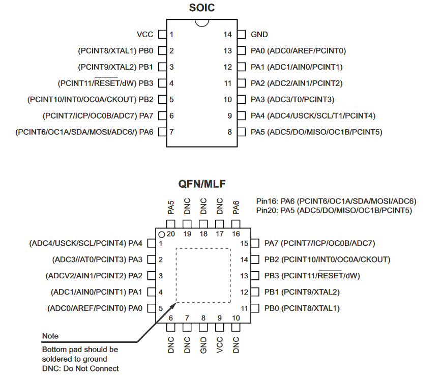
8-pins in total, 5 of them can be used for IO, plus another 1 pin can be selected for IO or dedicated RESET signal. However, I would not recommend using that pin for IO.
Although it is small, it comes with everything we may need. It has EEPROM and SRAM (and yes, some AVRs have no SRAM and you can only relies on the 32 or 16 registers to hold your data), two 8-bit timers, USI (I would like to call it semi- I2C and SPI), and ADC with differential gains.
The timer comes with a Dead time generator, which can be used to implement switch-mode power supply.
ATtiny25 features
The small dimension and low cost makes ATtiny25 perfect for some simple circuit, such as:
- I2C or SPI communication node.
- PWM signal generator, servo controller (require software to increase timer resolution).
- Switch-mode power supply.
- Simple programmable logic circuit.
- Simple programmable sensor.
- Replacement for legacy logic ICs such as NE555 and 74XX that becomes harder to source and more expensive to buy nowadays. Furthermore, it allows more flexible pin arrangement.
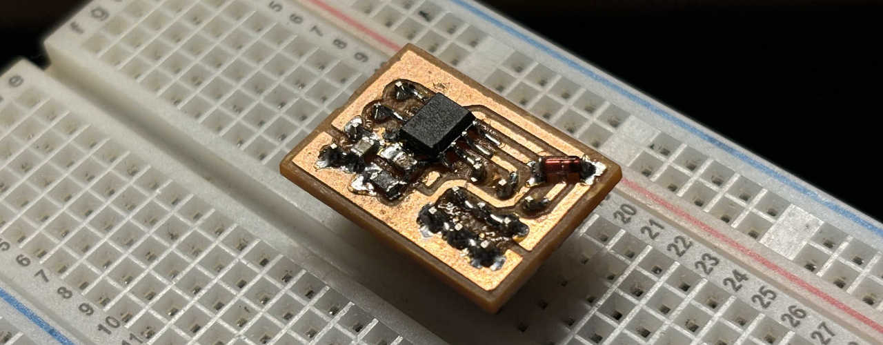
The above figure shows a 3 output servo controller using an ATtiny25 in SOIC package. In this design, the two USI pins are used to implement I2C communication; the other 3 pins are used for PWM signal (more precisely speaking, PPM signal) output. Because ATtiny only comes with 8-bit timers, it cannot generate PWM signal with 0.5ms to 2.5ms duty at 50Hz. Software is required to increase the resolution of the timers. However, this is a very simple embedded system, the CPU is powerful enough to deal with USI-based communication and high-precision PWM.
ATtiny24
ATtiny24 ATtiny44 ATtiny84
Highlights
Small size with 14 pins, 11 of them are IO pins, 1 of them can be selected as IO or dedicated RESET. (Samillerly, I would not recommend using that pin for IO.)
- 8 of the IOs are on PORTA to provide a full byte IO port. Furthermore, the pins are arranged in order, which allows us to connect PORTA to a parallel bus interface (like connect it to LCD1602).
- Among the 4 pins in PORTB, two of them can be used for external crystal to provide clock signal for the AVR, one can be used for RESET signal.
It comes with EEPROM, SRAM, a 8-bit timer and a 16-bit timer, USI for communication, ADC with differential gains.
ATtiny24 features
Compared to ATtiny25, ATtiny24 has slightly more pins and includes a 16-bit timer. This allows us to build a more complex system, such as:
- I2C or SPI communication node.
- PWM signal generator, servo controller (fully hardware).
- Slightly more complex programmable logic circuit.
- Slightly more complex programmable sensor.
- Replacement for legacy logic ICs such as NE555 and 74XX that becomes harder to source and more expensive to buy nowadays. Furthermore, it allows more flexible pin arrangement.
ATtiny441
ATtiny441 ATtiny841
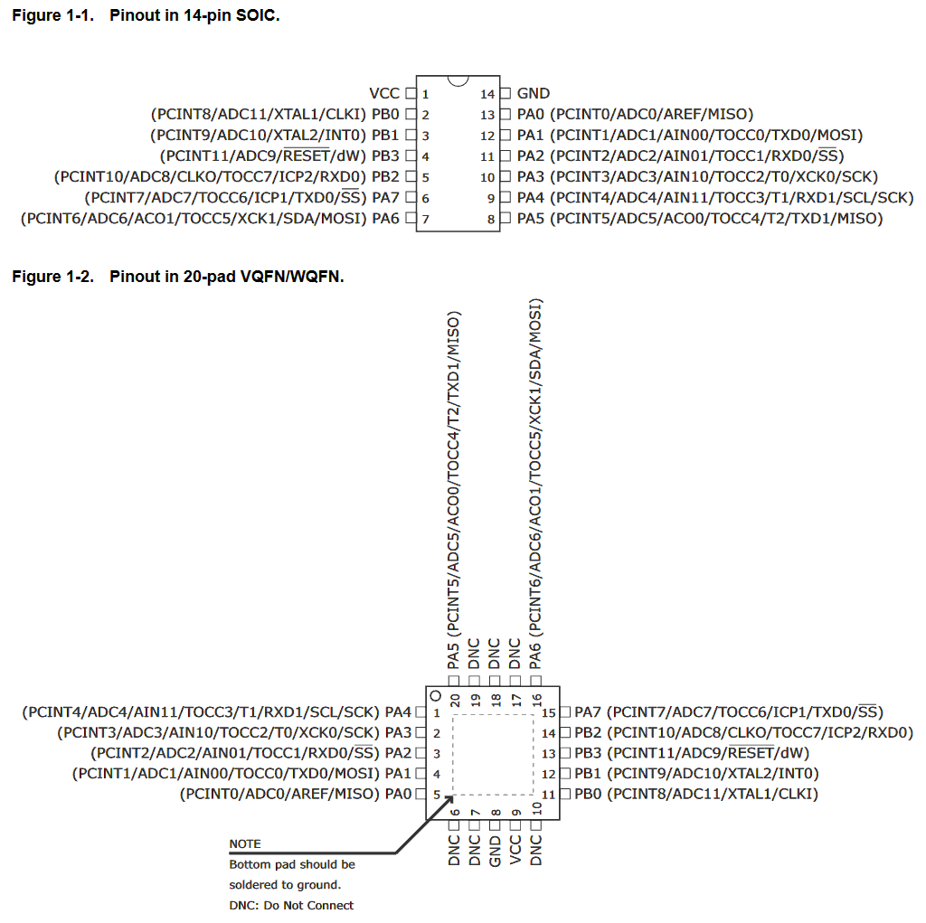
Highlights
As a drop-in replacement, ATtiny441 is fully compatible with ATtiny24's functionality and pin arrangement.
It comes with EEPROM and SRAM.
One 8-bit timer and one 16-bit timer. We can select the pins used for the timer output.
Two sets of analog comparators, and more options for ADC differential pairs and gains.
Two sets of UART/USART communication modules, one SPI communication module and one slave I2C communication module. We can select the pins used for the communication IO. Fully hardware communication support. (Software for USI is no longer required.)
Cons
Slightly more expensive than ATtiny24 (as of July 2024, Digikey shows ATtiny441 costs 10% more than ATtiny44). This may change as ATtiny24 may be phased out in the future.
No DIP package option. PCB or adapter will be required for people who use breadboards to build their circuit.
ATtiny441 features
As a more advanced version of ATtiny24, ATtiny441 has more hardwares inside. It allows more complex functionality with lesser code:
- Communication hub for UART, SPI and I2C.
- PWM signal generator, servo controller (fully hardware).
- Instruments with serial port interface.
ATtiny261
ATtiny261 ATtiny461 ATtiny861
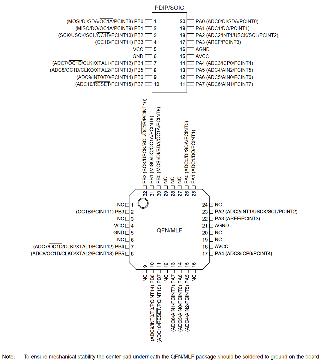
Highlights
As a drop-in replacement, ATtiny261 is fully compatible with ATtiny26's functionality and pin arrangement.(as of July 2024, Digikey shows ATtiny26 costs more than ATtiny261)
20 pins in total, 15 of them are IO pins, 1 of them can be selected as IO or dedicated RESET. (Samillerly, I would not recommend using that pin for IO.)
- One side of the chip is a power supply for the chip and ground, the other side of the chip is a power supply for analog and ground. The analog power supply should be connected to power no matter whether analog modules are used or not. My preference is to directly connect the power pins and ground pins on both sides of the chip when routing the PCB.
- PORTA is located on one side of the chip. All IOs on this side can be used as analog input; some pins can be used for USI.
- PORTB is located on the other side of the chip. Some IOs on this side can be used as analog input; some pins can be used for timer; some pins can be used for USI.
- Pins on both sides are arranged in their pin order in port.
It comes with EEPROM and SRAM.
One 8/16-bit timer and one 8/10-bit timer. The IOs support both positive output and negative output.
ADC with differential pairs and selectable gains.
USI with selectable output pins.
ATtiny261 features
ATtiny261 has even more pins for more complex functionality:
- I2C and SPI communication node.
- PWM signal generator, servo controller (fully hardware).
ATtiny2313
ATtiny2313 ATtiny4313
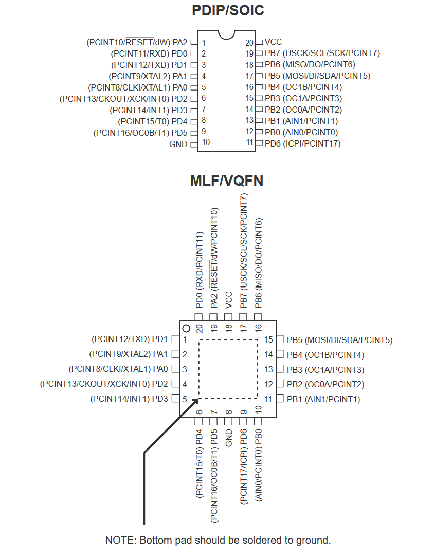
Compared to other ATtinys, ATtiny2313 comes with hardware USART for serial communication but lacks ADC for analog input.
I don't really like this chip, but there is no other ATtiny with hardware UART/USART in the DIP package. I would like to use software UART or use ATmega instead. If the SOIC package is acceptable, use ATtiny441.
ATtiny2313 features
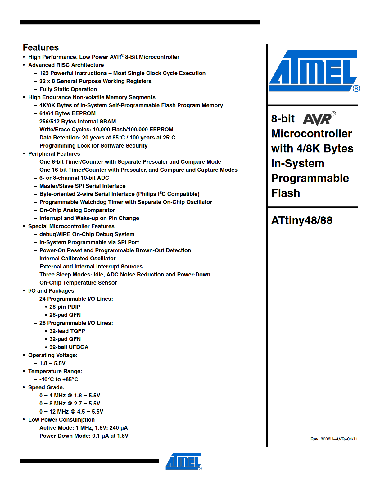
ATtiny48
ATtiny48 ATtiny88
ATmega48/88 without lots of sweet peripherals.
I don't really like this chip. I will use ATmega48/88 just to make my life eaiser. The cost difference doesn't justify it for me.
ATtiny48 features