Use CNC to make PCB
This blog shows how I use KiCad to design a PCB, then use FlatCAM to generate the G-code for a CNC to engrave on copper plated board. This blog also discusses the challenges I encountered and my solutions.
PCB, CNC, KiCad, FlatCAM, Embedded system, PCB prototyping, Gerber
--by Captdam @ Aug 31, 2024Index
When making a PCB, we will first design the path on a computer or paper, then make the physical PCB. There are computer softwares like KiCad that can help us create PCBs from schematics. This software can be used to generate Gerber files and that can be sent to professional PCB manufacturers; it can generate image files containing masks and can be printed on film for photolithography. Hardcore players can also choose hand drawn film without using any computer software, just for a joke :)
The above statement is a very common method for making PCBs and I believe there is a lot of literature available on the internet that can describe it better than me, and I don’t want to waste my time and your time to repeat that. Here, I am sharing my less common method: using CNC engraving and drilling. We will mill the circuit path on a copper-plated board and then drill holes for through hole components. I will also discuss the challenges I encountered and how I dealt with them.
Compared to photolithography, CNC engraving doesn’t involve any chemical; hence making our working environment less hazardous. It also imposes no timing and lighting restrictions. Furthermore, CNC can do both circuit path and hole drilling. However, CNC engraving needs more time and creates noise and dust. I think CNC engraving is suitable for small quantity fabrication and prototyping.
Design
Using Electronic Design Automation (EDA) software to convert schematics to PCB design and performing Design Rule Check (DRC)
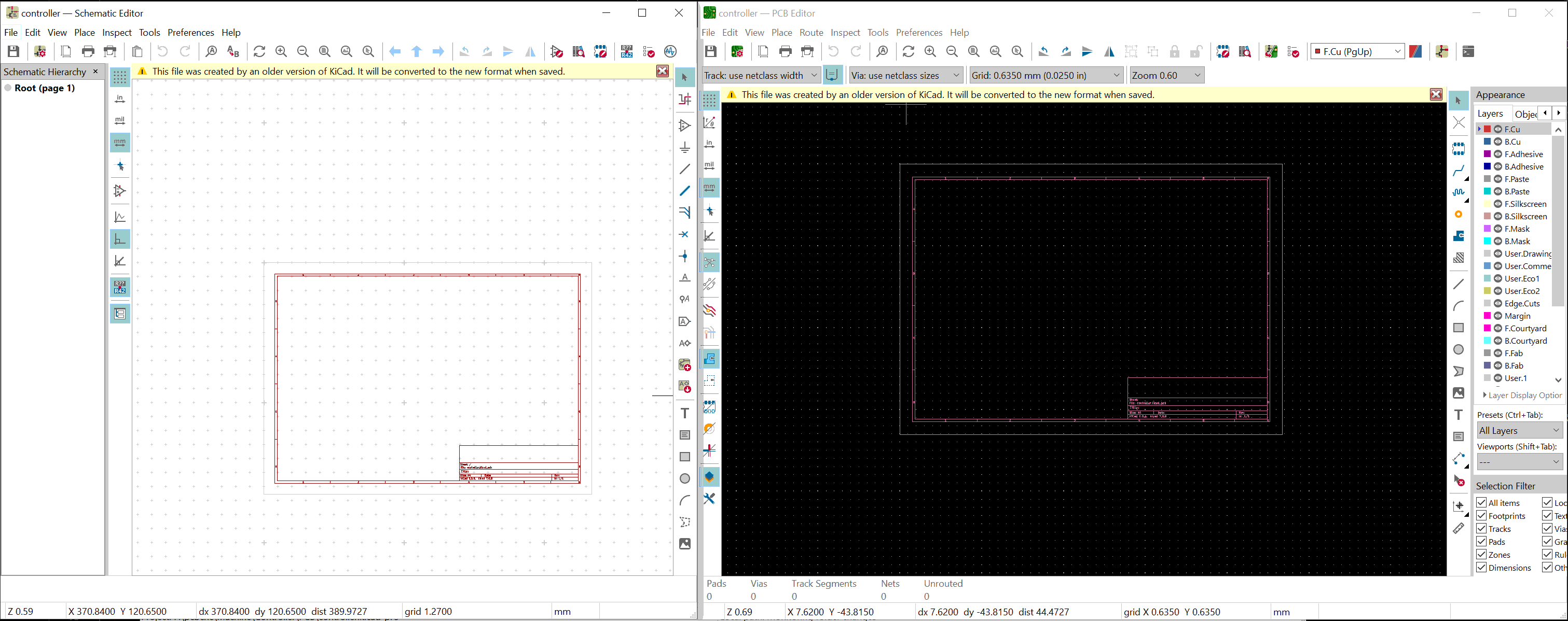
First of all, we will need to use EDA software to design the circuit. I am using the free and open-source software: KiCad。 KiCad provides almost everything we need to design a PCB. We can use this EDA software to create our schematic and then convert it into PCB design, and then to generate a Gerber file, an industry standard file that can be used to fabricate a PCB by professional PCB manufacturers.
We can also use other softwares. I am using KiCad because it is free and open-source, which is favored for individual developers like me. Development of KiCad is still active.
I have to mention that KiCad is not the solution for all cases. KiCad is PCB oriented, meaning it is used to create one single PCB. Therefore, it is not optimal if we need to make a system that has multiple PCBs. An example will be a system in a confined space where we have to divide circuit components into multiple PCBs, stacking the PCBs and use pin sockets for inter connections. We will have to manually divide the circuit components into multiple PCBs, create individual projects for each PCB, and manually make sure the size of each PCB and the location of pin sockets matches.
KiCad has a relatively complete library. However, when facing less common components (like some Chinese ICs), we will have to create our own library to instruct KiCad how to draw them on schematic and how to place them on PCB. Another solution is to use components that has similar pinouts.
Step One - Schematic Design
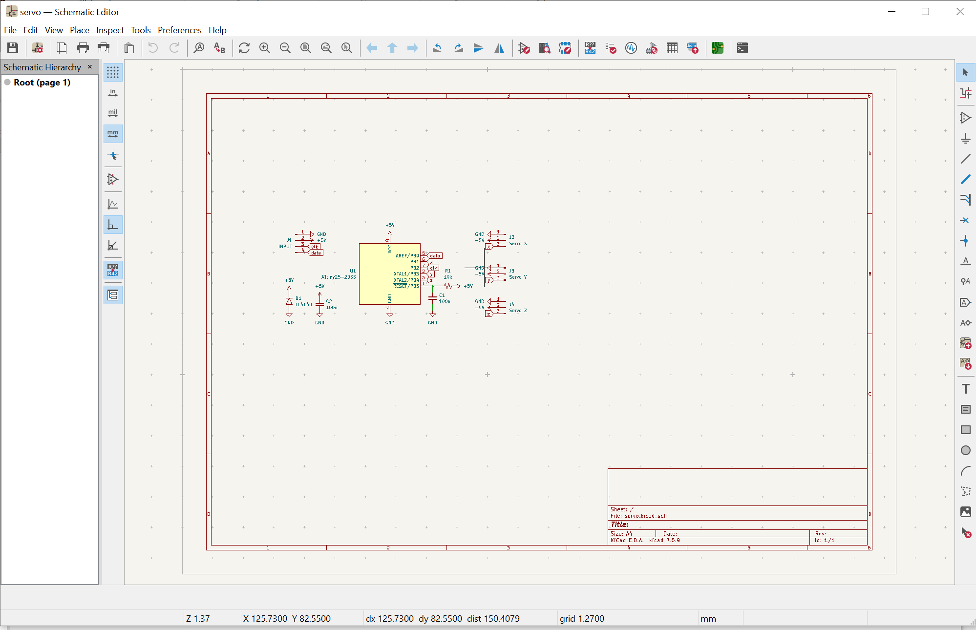
Let's draw a simple MCU system.
Place all components into the schematic and connect them together. When selecting the component, we need to select the package as well. For some components, such as MCU, the model number of the component indicates the package (For example, ATtiny441-SSU means ATtiny441 in SOIC package; while ATtiny441-MU means in MLF package). Some components, including basic resistors and capacitors, we will need to manually select the package. Some components don’t have a list of packages that we can choose from, we have to use a special category in the library to provide the package based on the package and the order of pinouts.
Although the mounting holes should not be part of the schematic (it does nothing to the conductivity of the circuit except grounding), we will have to insert mounting holes into the schematic editor. This is because when KiCad synchronizes the circuit from schematic editor to PCB editor, it will remove the mounting holes in PCB editor because there are no correspondence mounting holes in the schematic.
When inserting components into the schematic, if KiCad doesn’t automatically assign a number to them (in format of R?), we have to let KiCad assign the number. We can do it in horizontal order and vertical order, it is up to personal preference.
Nex, DRC. The purpose of this design rule check is to make sure all components are connected. It cannot detect bad circuit design (that’s for circuit simulation). It is worth mentioning that KiCad requires us to place PWR_FLAG on the power supplies, I don’t like this, I choose to ignore this category of error. When a pin is floating, we need to put an X on that pin to tell KiCad that pin is not connected.
My Preference
For components requiring high mechanical strength, such as pins, I would prefer to use through hole components. This provides the component on one side of the PCB, the metal pin going through the PCB and the soldering on the other side of the PCB. Together, they act like a revit pin on the PCB. If using SMD, external force may peel the copper layer off the board.
For components that are less likely to encounter external force, I will prefer SMD. SMD is smaller, cheaper and requires no through holes on the PCB. I normally use the 0805 package (0.8x0.5-inch or 2.0x1.2mm) for SMD resistors and capacitors. They are small but still good for hand soldering.
Different component types may share the same package. Interchange the component types doesn’t cause issues with PCB routing, but it affects the PCB rendering (for cosmetic). For example, if we select 0805 resistor for 0805 capacitor, when we render the PCB, we will see a resistor on our PCB instead of a capacitor. This is only for cosmetics since both have the exact same footprint on the PCB. If we don’t have the right footprint for one of our less common components and we don’t want to invest our time to add the right footprint for that component, using something else with a similar footprint is not a bad solution.
Step Two - PCB Design
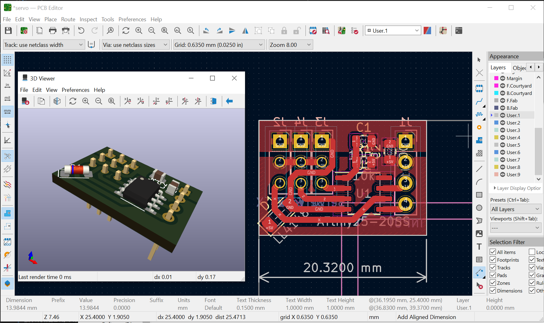
Update the schematic to the PCB. KiCad will tell us how to interconnect pins of components; furthermore, when we select a component in schematic editor or in PCB editor, KiCad will highlight the correspondence component in the other editor.
If we realize we need to go back to modify the schematic, we can go back to the schematic editor to modify the connection, the package, or to add or remove components. Once done, update the schematic to the PCB.
Before we make any connection, we need to design a list of trace widths we will use in the PCB editor. I would recommend add all possible trace widths we may use at once because KiCad is extremely lagging when updating that list.
After this, we can begin our routing process. We should use the top left corner as our origin (0, 0), this will be the origin of the generated Gerber file. Furthermore, we need to decide which side to place our components. For single-side PCB, we can place trace and SMD on the front side and place through hole components on the back side, or vice versa. Be sure to flip anything on the back side in CAM (in the next step).
We can define a filled zone, so KiCad will fill that area with a circuit pole. One common way is to define the entire board to be a filled zone for GND.We can also define different area to be filled with different poles, like the power supply on one side of the PCB and GND on the other side of the PCB. We can also define a Do not fill zone, this rule is common on high voltage circuits and RF circuits. If we define a filled zone for GND, we can ignore all GND connections when we route the traces for now. After we finish all other traces, we will run the DRC and KiCad will fill the zone for us. In the figure, we can see a filled zone for power supply and a filled zone for GND in shadow.
After DRC, KiCad will tell us missing and wrong connections and courtyards overlap. We can also render the PCB in 3D viewer to preview the PCB. If we are going to hand solder all components, we can ignore courtyard overlap errors.
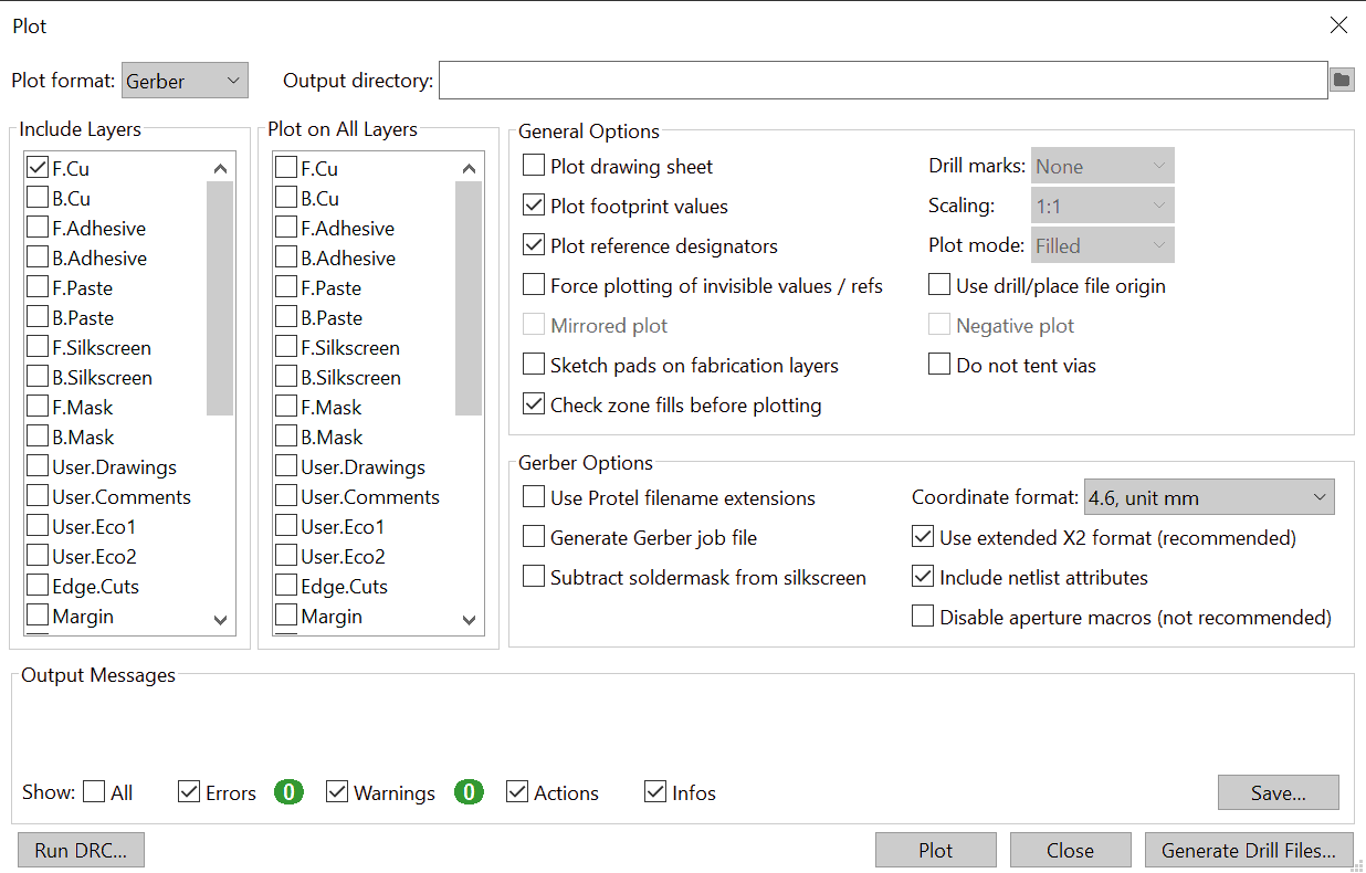
Finally, we can export the PCb design. We will have two types of files: grb files for traces and drl files for holes.
My Preference
When placing components, we will snap components on the grid. I prefer to use a 0.025-inch grid, which is a quarter of the pitch of DIP components.
If we add new components, we should not reassign numbers to components that are already in the PCB designer. KiCad corresponds components in PCB editors and components in schematics editor by their number. If reassigned, KiCad will lose track of them.
Thicker traces are preferred because of less resistance. I normally give the power supply more than 1mm width. Devices requiring a large amount of current will have an even thicker trace or filled zone.
For trace carry signals, I will use 0.45mm or higher width. If the trace is long, a wider trace will be favored. Because my CNC uses a V-shape mill bit and the bed cannot be not perfectly leveled, there will be error between the specific trace size and the actual trace size, and the trace size may differ at different locations of the PCB. For the clearance between traces, I use 0.2mm (slightly smaller than the 0.007-inch setting I used in the next step). With 0.45mm trace size and 0.2mm clearance, I can create a feature size of 0.65mm. In other words, that allows me to run a trace between two pins of the SOIC package.
For soldering pad and Via, I will use 0.1mm maximum hole size and 1.3mm minimum pad size, this will give sufficient area to solder a pin on the pad while allowing one trace to run between two pads of a DPI package. We can also use rectangular pad instead of the default circle pad to increase pad area to allow better soldering.
Because I am using CNC to engrave PCB, I can only make single size or double side PCBs. Making double side PCBs requires aligning the PCB after flipping it, which is inconvenient. Therefore, I only make single side PCBs. We can run most of our traces on one side, and use the other side for the bridges; therefore, we don’t need to specifically insert meter wires for the bridges.
Because I only make a single side PCB, I will only need one Gerber file the the side I run my traces and one drill file for my holes.
Prepare
Converting PCB files into G-code for CNC
We will need Computer-Aided Manufacturing (CAM) software to convert PCB fabrication files into G-code that CNC understands. Once again, I will use free open-source software: FlatCAM. Installing this software is not very convenient. I am using version 8.5; the newer version, 8.6, to my opinion, is not easy to use.
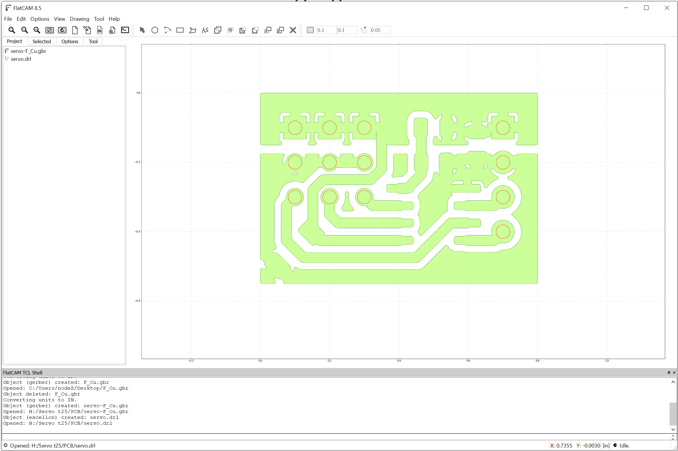
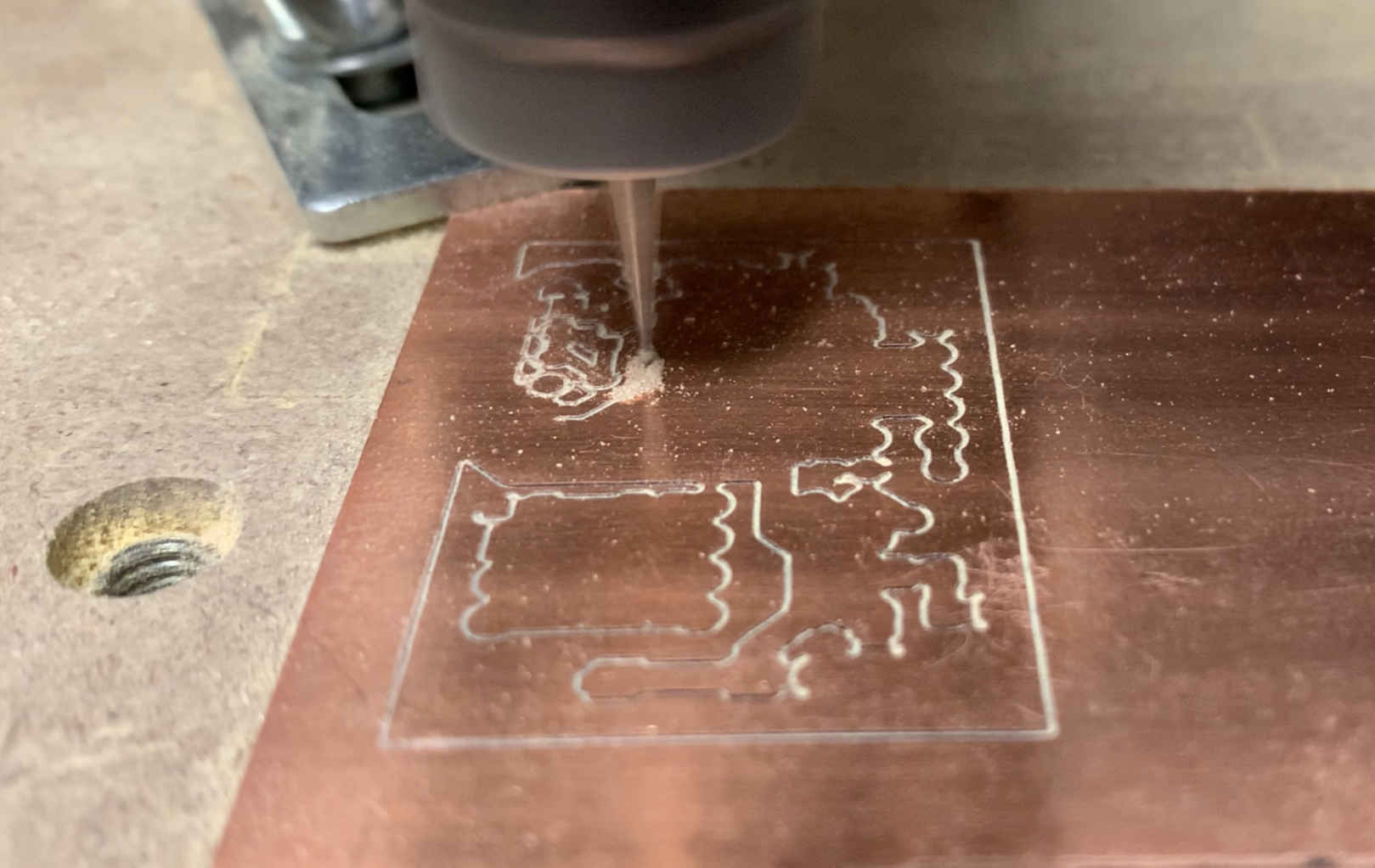
Step One - Isolation
Import the Gerber and Drill files. If the Gerber contains traces on the back side, we will need to flip it because CNC engraving happens on the front side.
Isolation, which is to isolate different traces by engraving the clearance area of the PCB, is the most important step in the fabrication. During the design, if the clearance is too narrow, the mill bits won’t be able to pass through it. In other words, isolation will fail and traces on PCB will be short. If we only have one or two short circuits on the PCB, we can use a knife to post-process it; otherwise, we have to go back to the PCB editor to increase the clearance.
My setting:
- Toll size: 0.007-inch
- One pass only.
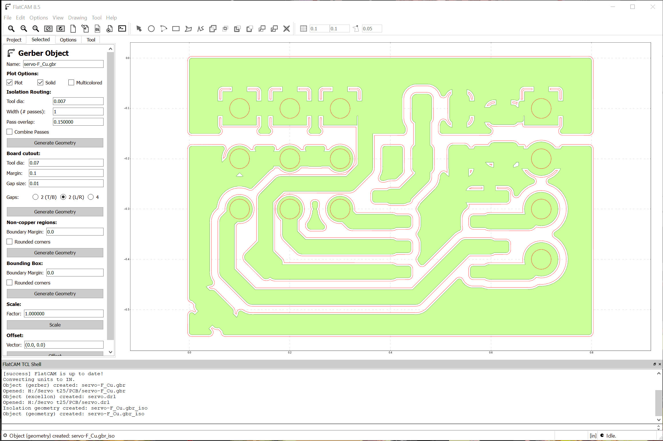
Now, we can see the mill routes in red and circuit traces in green. We need to ensure that the mill routes completely isolate the circuit traces. If we zoom in the above figure, we can see some place has not been isolated; however, they won't cause any short circuit so we are fine.
Next, we need to configure the mill (cut) depth, travel height and cut speed.
My setting:
- Cut Z: 0. We will setup the CNC so 0 height is the height just cut through the copper layer of the board.
- Travel Z: 0.025-inch.
- Feed rate:0.5. Due to large drag force, slower feed rate can reduce load on mill bit; hence prevent hockey stick issue.
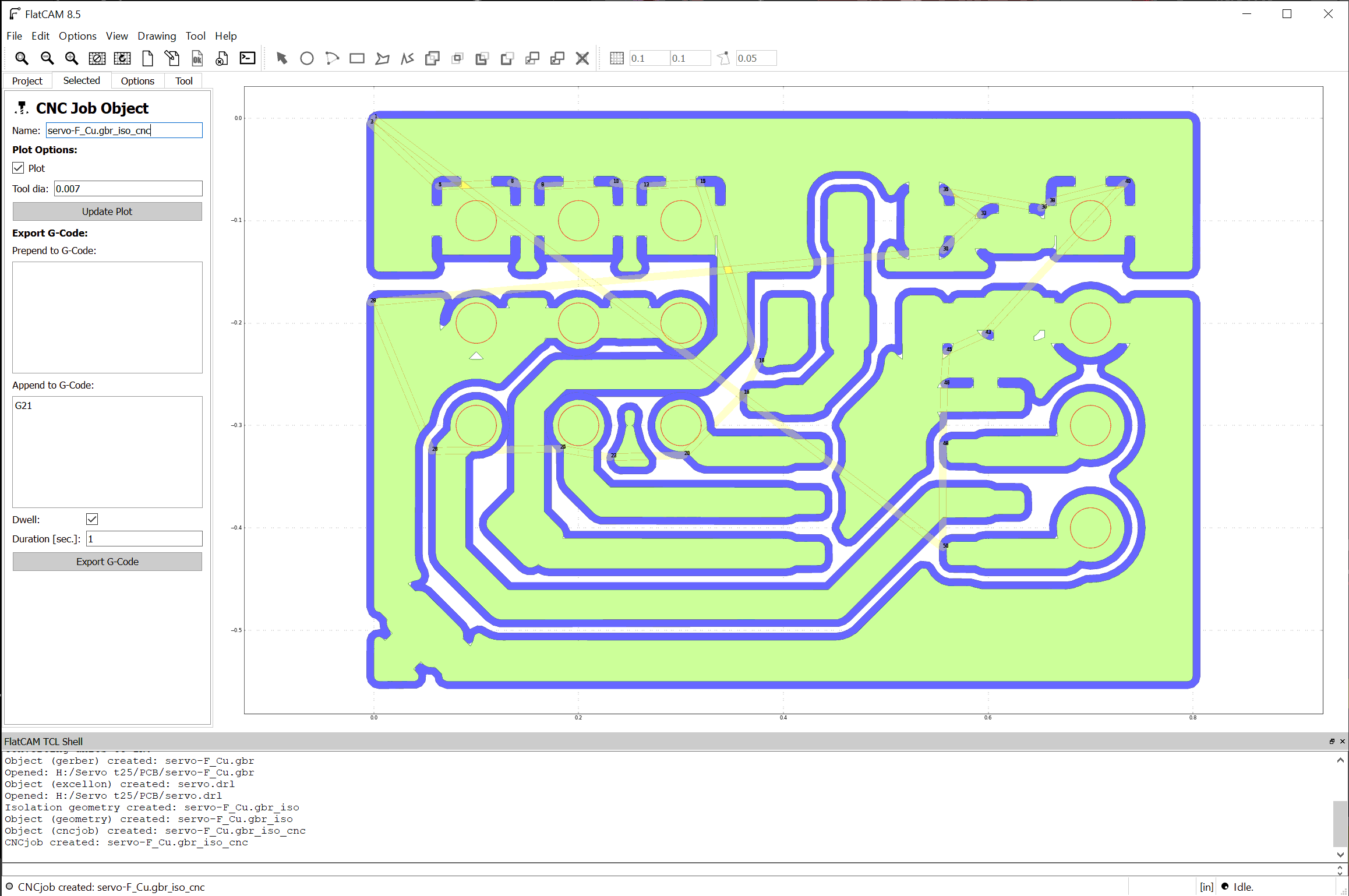
At the end, generate the G-code. We can add a G21 instruction at the end so the CNC go back to mm mode.
Step Two - Drill
If there are any through hole components in our circuit, we need to drill the holes for them.
Because our CNC is one of the most basic models, it cannot change tools by itself. We will treat all holes the same size. In other words, we are using one 0.3mm drill bit for all hole sizes. This drill size should be good in most cases; if we encounter components with large insert pins, we will manually drill them afterwards using larger drill bits.
My setting:
- Cut Z: -0.055, which is a little bit thicked than the PCB thickness.
- Travel Z: 0.025-inch.
- Feed rate: 0.5, to prevent snap drill bit.
Step Three - Cutout
Now, we can take our finished PCB out from the big plate. We can let FlatCAM generate a cut out box for us; or to export the Edge.Cuts layer from KiCad.
If we let FlatCAM generate a cut out box for us, we need to tell FlatCAM the margin distance we want between cut out box to circuit traces.
If we use the Edge.Cuts layer from KiCad, there is a trick. Because KiCad exports the Edge.Cuts layer in a Gerber file, FlatCAM will mistakenly recognize it as a circuit trace. We will use the same method we used in isolation; but, we will change the tool size to negative number and increase the cut depth. In this way, we can mill on the trace instead of out of the trace.
My setting:
- Cut Z: -0.055, which is a little bit thicked than the PCB thickness.
- Travel Z: 0.025-inch.
- Feed rate: 0.5 or lower. Similar to isolation but deeper cut than isolation.
CNC Engraving
Using CNC to engrave traces and copper-plated board and drill holes for through hole components
Finally, we are ready for making the physical PCB!
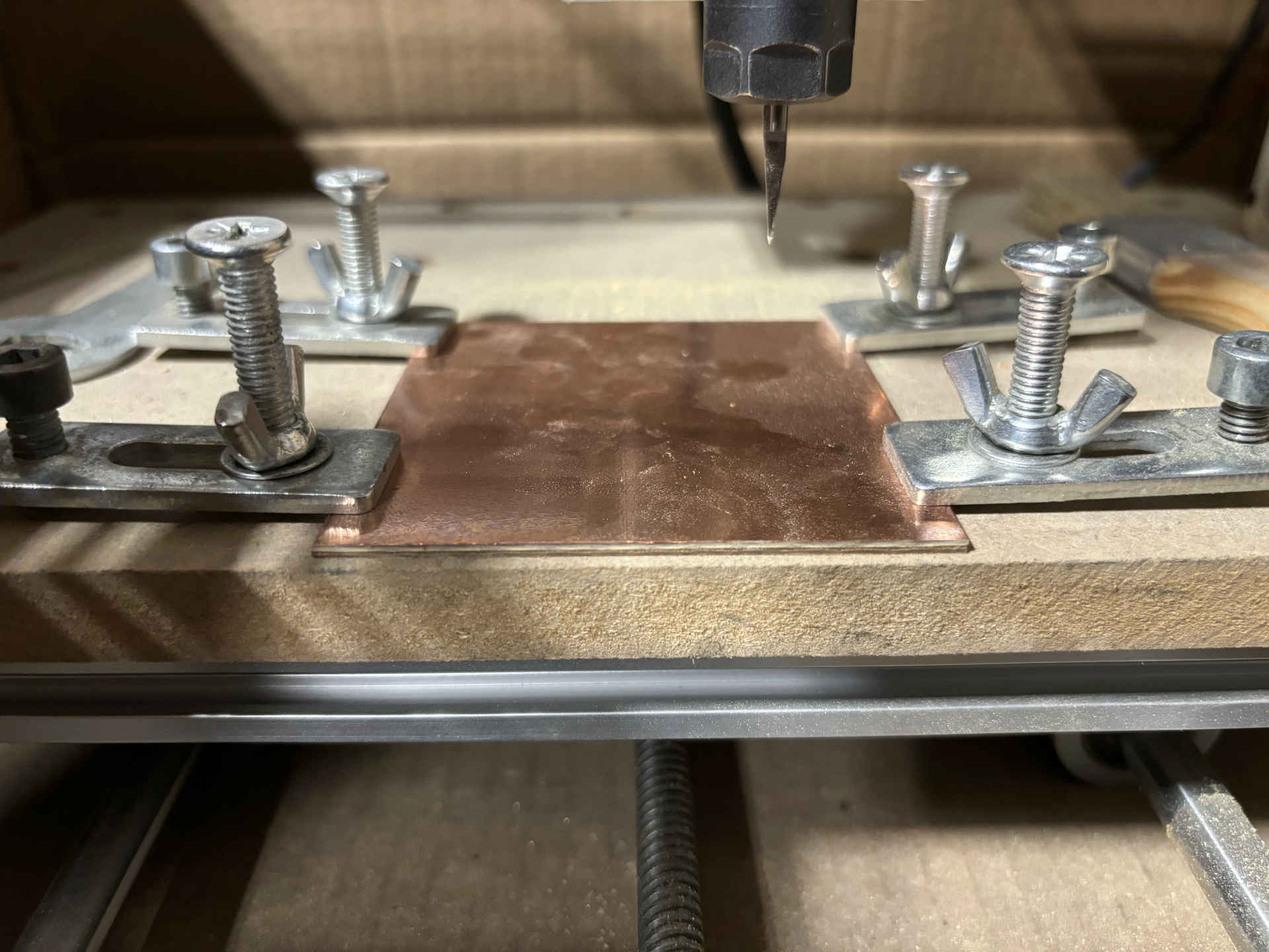
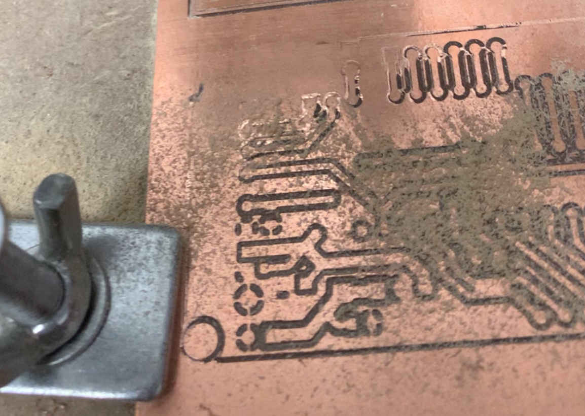
Place the copper-plated board on the CNC bed using clamping tools. We must ensure the bed is level and the clamping tool is not compressing and warping the board. I usually press the board down towards the bed when I install the clamping tool.
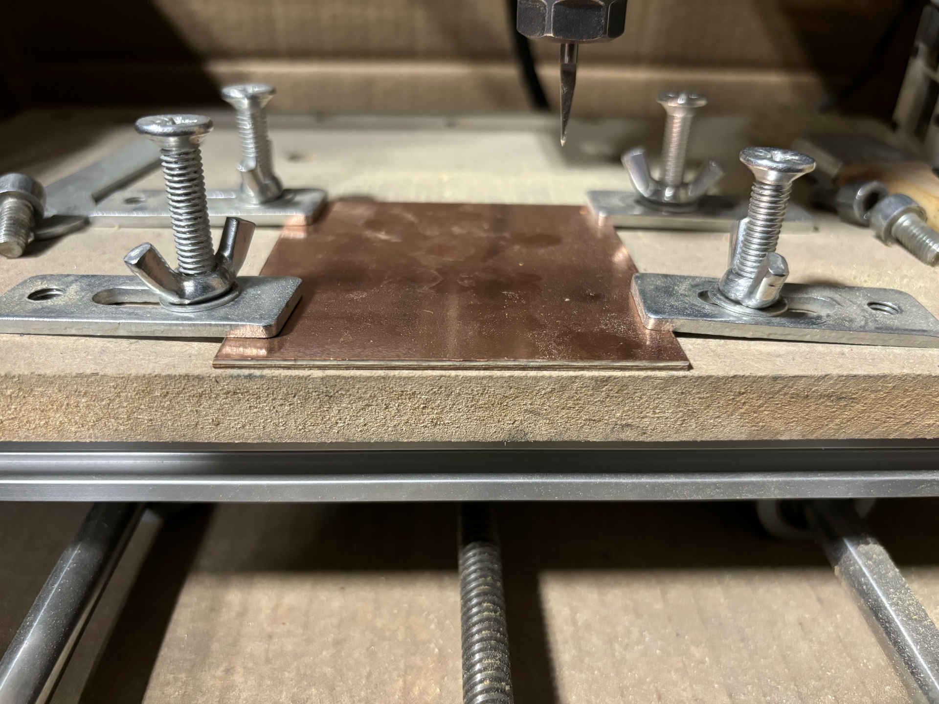
The figure shows a wrong installation of the clamping tool. In this setup, the clamping tool will compress the board. The result is that the board will warp in the middle, illustrated in the following figure.

The correct way is to place a spacer on the other side of the clamping tools to eliminate any inwards forces.
Furthermore, due to the V shape of the milling bit, the cut width will not be consistent at different locations if the bed is not leveled.
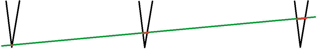
Following is examples of an unleveled bed. As we can see, the traces on the top left corner are not completely isolated. This will short our circuit.
This issue can be solved by calibrating the bed. However, it may not be practical in some cases. One way is to add Z-axis in the G-code so the mill bits change height as the board surface changes height. Another way is to reduce PCB size to minimize the negative effect. This is one of the reason I prefer small-size SMD components and small PCBs.
Now, we need to calibrate the mill bit. We first move the mill bit to the place above the origin of the PCB (plus some clearance). Slowly (I mean, really slow, or we may break the mill bit) lower the mill bit until it contacts the copper plate. Because both the mill bit and the copper plated board are conductors, we can use the conductivity between the mill bit and the board to indicate that the bit touches the board. Another way is to turn on the spindle motor and feel the vibration on the board from the mill bit when they get in contact. We will lower the mill bit by an additional 0.1mm, which should be sufficient depth to isolate 1-2 oz copper.
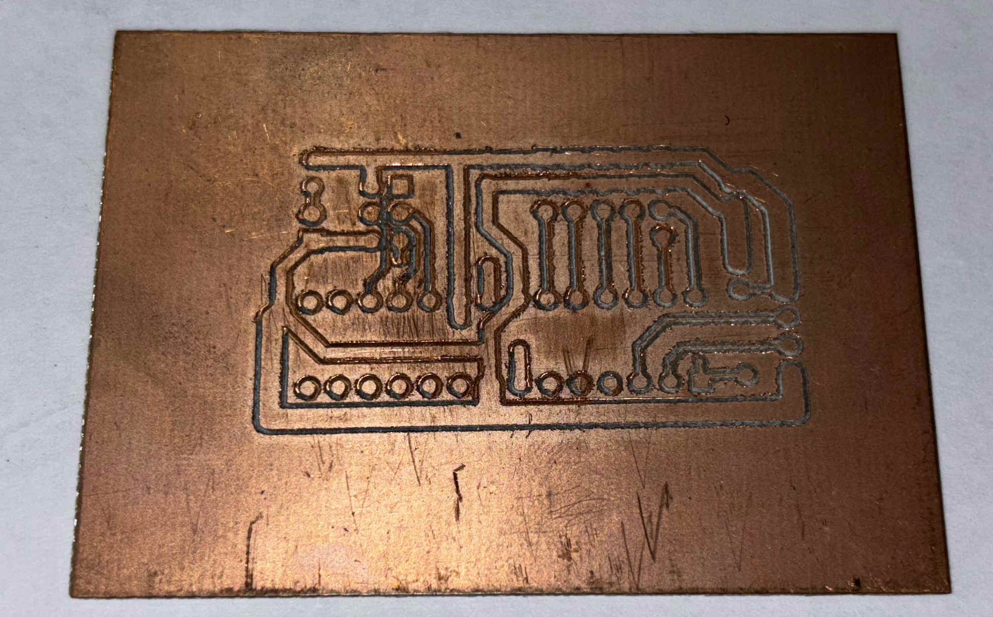
Before we put any mill on the board, we can examine the mill depth by checking the mill width. To do so, we will instruct the CNC to move the spindle in horizontal directions in a small test region. We should look for the depth that just cut through the copper layer. This not only provides thicker circuit traces (hence, less resistance and less chance of broken traces); but also reduces wear on milling bits. However, considering the reliability of the cut and the possibility of unlevel bed / board, deeper cuts may be required. If we realized that we are milling too shallow after we finish the process, we can do a second mill pass.
Following photo shows a PCB in 3 different mill depths. As we can see, the left one has the shallowest mill and provides a very clean PCB. The middle one has moderate depth, it is favored for larger size PCBs. The right one is way too deep, and it looks nasty.
We should fabricate our PCB in the following order:
- Isolation: This step is extremely strict on the mill depth, it requires us to calibrate the mill bit(as mentioned above) on a clean (new) copper plated board surface. Furthermore, this step is crucial for the final quality of the PCB. If this step fails, there is no need to continue in the following steps.
- Drill: This step is required if we use through hole components only. We need to replace the mill bit by drill bit in this step and calibrate the drill bit. Once done, we need to change the tool back to mill bit for cut out. Since we are drill through in this step and cut through in the next step, we don’t really need to accurately calibrate the tools. However, it is still inconvenient to change tools twice; therefore, I prefer to design PCBs with SMD only to avoid this step.
- Cut out: to remove the PCB from the board.
Finish up
Install the components and soldering
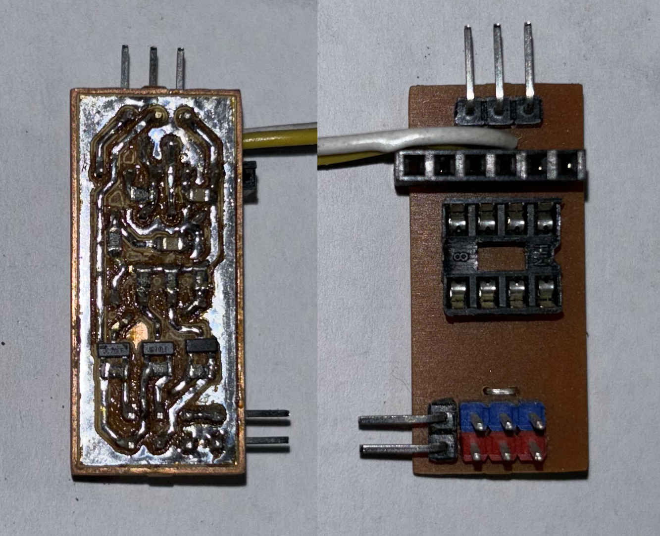
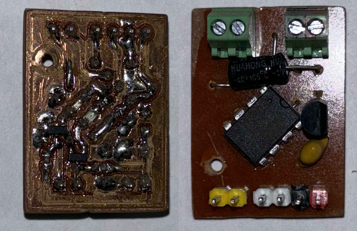
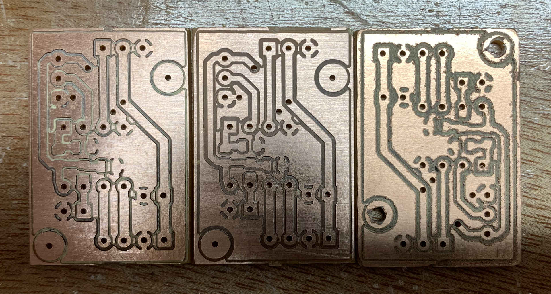
Let's end this blog by some finished PCBs.
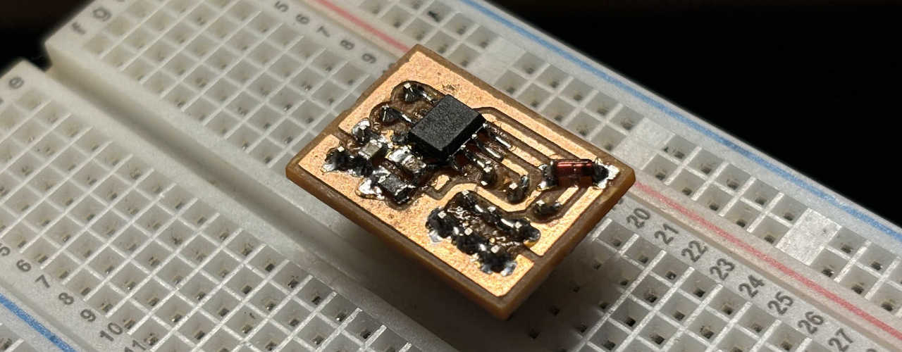
Following photoes shows the front and back side of the PCBs: