NMOS and diode based level shifter design
Introduce two different level shifter for logic circuit design: the NMOS-based design and the diode-based design. This blog will introduce the working principle of both design, provide PCB layout for both of them using SMD, provide timing diagrams using scope for both implementation, and compare the pros and cons of them.
Level shifter, Embedded system, voltage, NMOS, diode, 2N7002, LL4148, circuit design, PCB layout
--by Captdam @ Dec 23, 2023Introduction
It is common to encounter issues that two components are working in different voltage when designing a logic system. For example, some sensors are working at 3.3V but MCUs are working at 5V. If directly connecting them together, the low-voltage device may not be able to withstand the higher voltage and will be damaged. Some low-voltage devices have high voltage-tolerance IO (for example, the W5500 Ethernet chip works at 3.3V but allows digital IO up to 6V).
One of the solutions is to use level shifters. There are level-shifter ICs and modules can be use; however, sometimes it makes more sense to use discrete components to implement level shifters as it provides more flexibility in design, is easier to get, has lower price than ICs; and consumes less area than modules.
This blog will introduce two different level shifters for logic circuit design: the NMOS-based design and the diode-based design. This blog will introduce the working principle of both designs, provide PCB layout for both of them using SMD, provide timing diagrams using scope for both implementations, and compare the pros and cons of them.
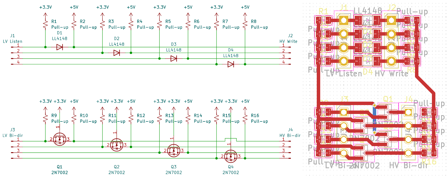
Above is the schematics and the PCB layouts of both designs with 4 channels each. Both designs use the most common (and lowest price) devices: the LL4148 SMD diode and the 2N7002 SMD NMOS. If use through hole device, 1N4001 diode and 2N7000 NMOS.
In the above schematics, we used 5V to represent the high-voltage system and 3.3V to represent the low-voltage system. We will use the same notation in the following text. Both designs should work for systems with other voltage as long as the voltage is within the voltage range of the diode / NMOS (Gate-source voltage for NMOS).
Pull-up resistor is required on the listening side. Pull-up resistor can be removed on the write side if the write side uses push-pull type output, but required if it uses open-drain type output.
Diode-based Design
Diode only allows current flow in one direction, that is, from high-voltage side to low-voltage side. In the design shown in this schematic, we place the diode in the direction that it allows current flow from low-voltage listen side to high-voltage write side, but forbid current flow in the opposite way; hence protect the system on the low-voltage listen side from high voltage. Consider the following cases:
When the high-voltage side outputs 5V, current cannot flow through the diode; therefore, the pull-up resistor on low-voltage side pulls the line to 3.3V.
When the high-voltage side outputs 0V, current can flow through the diode; therefore, the diode will drain the voltage on the low-voltage side to 0V. In this case, there will be some current leaks through the pull-up resistor.
It is very easy to route this design on single-side PCB using with SMD diodes, as shown in the above PCB layout.
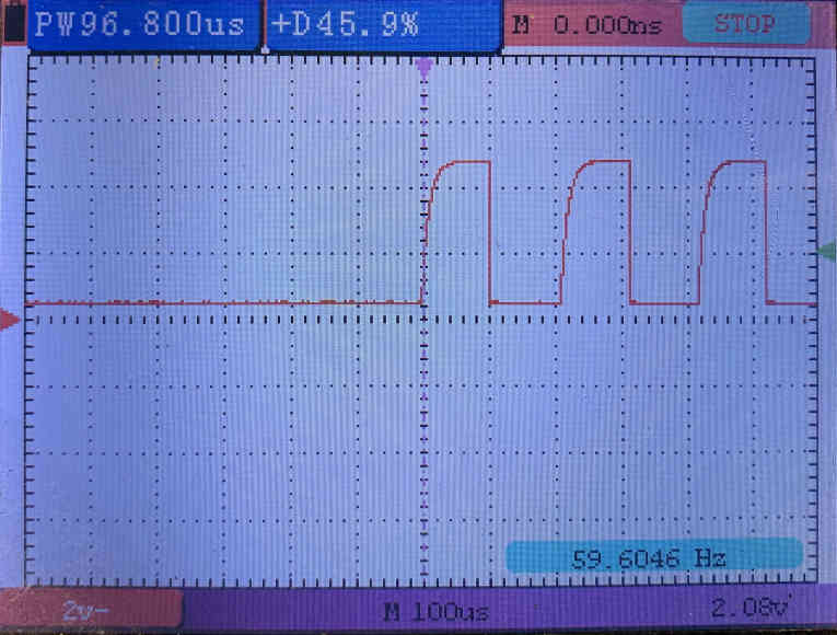
When the signal on the high-voltage write side changes from 0 to 1, current cannot flow from the high-voltage write side to the low-voltage listen side. Charges must be filled onto the line by the pull-up resistor. Due to the resistance of the pull-up resistor and the capacitance of the line, the charge filling process could take a while. This results in a slow voltage rising-up on the low-voltage side. The timing diagram shows the signal wave drive by a 5V push-pull type MCU output and a LL4148 diode. With 47k ohms pull-up resistor, the rise time is about 40us. When outputs 1, power of this circuit should be zero; when outputs 0, this circuit will draw about 5 X 0.1mA = 0.5mW.
The rise up time can be reduced by decrease the resistance of the pull-up resistor, but will result in higher power consumption when the high-voltage side outputs 0. A low-speed system may choose higher resistance value to save power; high-speed system may focus on low rise time instead of power saving.
Due to the voltage drop of the diode, the voltage on the low-voltage side will not reach real 0V. When the voltage on the high-voltage write side is 0V, the voltage on the low-voltage listen side will be the drop voltage of the diode. For most diodes, this value will be around 0.5V (this value should be safe for most digital devices. But, always check the input low voltage for the target device to confirm it). Furthermore, the drop voltage of the diode increases when the current increases. Therefore, it makes more sense to uses a higher resistance value for the pull-up resistor because it allows less current, which means lower drop voltage on the diode.
Pros:
Very simple design, and very low cost.
Withstand very high voltage (50V for 1N4001, 1kV for 1N4007!).
Simple PCB routing.
Cons:
Signal only flow from high-voltage side to low-voltage side.
Slow pull-up or high power consumption.
Low-voltage side will never reach 0V.
Low-voltage side must not write. Short circuit if low-voltage side writes 1 when high-voltage side writes 0.
NMOS-based Design
The NMOS design works by utilized the hall effect and the built-in diode of the NMOS: Current can flow through the hall in both direction when Vgs (Gate-source voltage) is greater than the threshold for NMOS, and in the direction of the diode at all time.
In this design, since gate is fixed to the power supply of the low-voltage side, current can flow through the NMOS when the low-voltage side is 0V. On the other hand, current can also flow from the low-voltage side to the high-voltage side through the diode.
There are four cases to study for this design:
Both the high voltage side and low voltage side writes 1. Vgs is 0V, hence no current flow through the hall. There is no current flow through the diode as well since the dirrection of voltage difference is opposite of the diode direction.
Both the high voltage side and low voltage side writes 0. Current can flow through the hall because Vgs is 3.3V. Although no actual current flow in the hall because both sides are 0V.
The low-voltage side writes 0. Vgs is 3.3V, current can flow from the high-voltage to the low-voltage side through the hall. The high-voltage pulled down to 0.
The high-voltage side writes 0. current can flow from the low-voltage to the high-voltage side through the diode. The high-voltage side pulls down the line on the low-voltage pulled to 0. At this moment, voltage on the low voltage side will be the drop-down voltage of the internal diode, which is almost 0V. This causes the Vgs to be greater than the threshold, which opens the hall and allows current to pass through the hall as well. Now, current then flow through both the hall and the diode. Unlike the diode-based design, the hall has (almost) no drop voltage and allows the voltage to reach (almost) true 0V.
There are two cases to study for this design if the devices use push-pull type outputs:
The high-voltage side writes 1 but low-voltage side writes 0: Vgs is greater than threshold, current flow from 5V high-voltage side to 0V low-voltage side, short circuit.
The high-voltage side writes 0 but low-voltage side writes 1: current can flow through the built-in diode, short circuit.
Detail description of this design can be found in Application note AN97055.
Routing of this design requires connecting the NMOS to power supply of the low-voltage side. This imposes some challenges on single-side PCB.
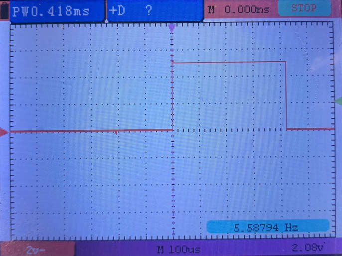
As the timing diagram shows, the NMOS-based provides better performance than the diode-based design when the signal change from 0 to 1. The timing diagram shows the signal wave drive by a 5V push-pull type MCU output and a 2N7002 NMOS. Even with 47k ohms pull-up resistor, the circuit response to the input change with less than 1us delay. Unlike the diode-based design, the NMOS-based design is bidirectional, which introduce two more current path other tahn the pull-up resistor:
The high-voltage side changes from 0 to 1 and low-voltage is still at 0V: In addition to the pull-up resistor on the low-voltage side, current can flow from the high-voltage side to the low-voltage side through the hall until Vgs becomes less than the threshold.
The low-voltage side changes from 0 to 1 and high-voltage side is still 0V: In addition to the pull-up resistor on the high-voltage side, current can flow from the low-voltage side to the high-voltage side through the diode until voltage on the high-voltage side becomes higher than the low-voltage side.
This design allows the voltage on both side to be pulled to 0V by the other side because the current can pass through the hall.
Pros:
Faster pull-up.
True 0V.
Cons:
NMOS needs to be connected to power supply of the low-voltage side, hard to route on single-side PCB.
Slightly higher cost.
NMOS has lower voltage rating than diode.
Short circuit if one side writes 0, the other side is push-pull type and writes 1.